


Other Parts Discussed in Thread: TPS84259
Tool/software:
Hello.
It contains 4x TPS84250 and 4x TPS84259.
The four TPS84250 outputs are set to +11.5V, because I connected a 133K 0.1% resistor between VOUT and VADJ, which is the pin 36.
The four TPS84259 outputs are set to -11.5V, because I connected a 133K 0.1% resistor between VOUT and VADJ, which is the pin 36.
For all cases the input voltage is +24V, and there is a schottky diode from this +24V to the input of each chip.
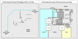
I created this topic looking for a review of layout of the TPS84250 first. There are four power supplies using it, I did the layout of it one time, and I would like to validate it, then later I will do a copy for the other three.
The simplified stack of the PCB, only considering the copper layers, is:
L1: Top
L2: Ground plane
L3: Power plane. Multiple +11.5V planes
L4: Power plane. Multiple -11.5V planes
L5: Ground plane
L6: Signals + ground
L7: Ground plane
L8: Bottom
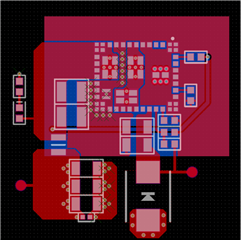
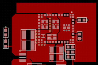
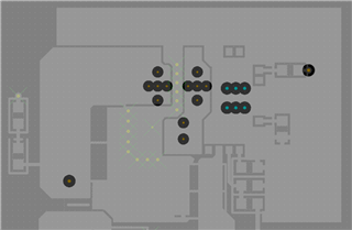
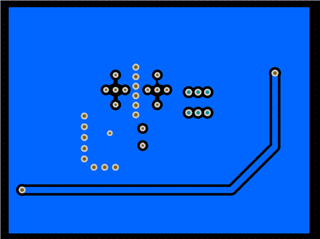
Below are pictures of my layout. Below is not shown how is L6, but in L6 at the chip area there will be a ground fill, similar to L8, bottom, but enlarged.
General view:
L1, Top:
L2 and L5 and L7, Ground planes:
L8, Bottom:
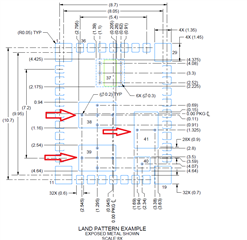
The picture below is shown in the page 23 of the datasheet, I have rotated it 180 to match the orientation of my layout.
The picture above seems to not consider the holes of the picture below, which is shown in the page 34 of the datasheet, which are over the inner pads of PH and VOUT, and that is why my ground planes have more openings.
Regards.
