Because of the Thanksgiving holiday in the U.S., TI E2E™ design support forum responses may be delayed from November 25 through December 2. Thank you for your patience.

MC33063A-Q1: Absolute MAX Swtich current

Part Number: MC33063A-Q1
Other Parts Discussed in Thread: MC33063A, LM51581, LM5157, LM5158, TINA-TI

Tool/software:

Hi Team,

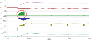
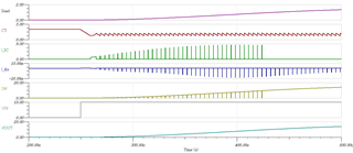
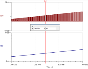
I have question about the switch current for the MC33063-Q1. Accouding to the datasheet, the switch current max value is 1.5A right. when I see the simulation result at TINA TI, I can see the value is over the 1.5A like as below. Is it acceptable? If so, how do we understand this results? 
Best Regards,

Uchihara

  • Hello Uchihara, 

    Thanks for reaching out to us via e2e.  

    As you can see on our product website, the TINA model is not (or no longer) available there. 

    The only official model is the PSpice model. 

    In other words, the TINA model is no longer supported, and we do not have the bandwidth to deal with it. 
    We can neither comment on any short
    comings of the TINA model, nor fix it.


    Therefore, may I please ask you to use the PSpice model instead, as this is the only version where we can get help, if necessary. 

    Please also make sure that you will use PSpice for TI or a full blown PSpice simulation tool for it.
    Tools from other vendors, e.g. LTSpice are not fully compatible and may not work properly either. 
    Please understand that we cannot support problems with third party tools.

    Best regards

    Harry

  • Hi Harry,

    Customer also see similar issue on thier bench. Can you share any thought? there is no possiblity to happen this issue?

    Regards,

    Uchihara

  • Hello Uchihara, 

    I think I understand your problem now. 

    The MC33063A is a very primitive device.

    It does NOT have any built-in current limit circuitry to protect the internal transistor. 


    You need to calculate all external components (including the sense resistor) according to the equations in chapter 9.2.1.2 of the datasheet. 

    All that can happen is that the comparator will turn off before the max current is reached. But this comparator cannot see the actual current through the transistor. 

    So, all components have to be calculated carefully and if the load is too high you may not be able to build a proper system, and the internal transistor may see too much current and overheat. 


    Why don`t you propose using the much more modern LM51581 instead?

    LM5157 / LM51571 / LM5158 / LM51581 are all one series of asynchronous converters with built-in FET. They offer different current and voltage levels. 
    The cense resistor is internal and cannot be adjusted. 
    Therefore, please select the one where the expected peak current is in range. Do NOT simply select the part with the highest current rating, otherwise there will be no proper regulation. 

    The LM5157/8 family also comes with a QuickStart calculator which will help to calculate the external components like the inductor.


    Best regards

    Harry

  • Hi Harry,

    Thank you for your answer. It's already production and face the PCN.

    Customer caluculate the Rsc value using below fomula.

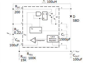
    Currently they set the Ipeak = ISW_Abs_Max=1.5A Therefore they set the Rsc value bigger than 0.2. Acutally 0.22 ohm like as below. Is it acceptable?

    Regards,

    Uchihara

  • Hello Uchihara, 

    Yes, this should work.
    In reality there is some reaction time where the inductor current still keeps rising before the transistor gets turned off.
    So the resulting current may be a little bit higher than calculated.


    Best regards
    Harry

  • Hi Harry,

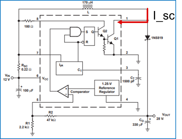
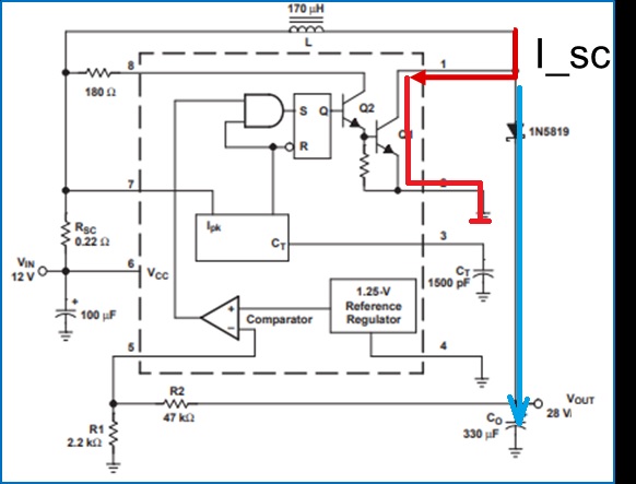
    Thank you for your reply. Let me make sure my understanding. The switch current of the datasheet means same like as below fiture. Is it correct?

    If so, the I_SC actual value is violated to the AbsMax value > 1.5A at a start up timing. I think even though we carefully calculate the discrete parameter, lt's not possible to avoid the I_SC > 1.5A. Because the output capacitor lead to inrush current and I_SC turn on time is depeding on the CT charging time. If VCC>3V, the SW will be started right? Can we ignore the start up period even thoguh the absmax >1.5V because it's very short time?

    Best Regards,

    Uchihara

  • Hello Uchihara, 

    Yes, the switch current is the current going across Q1. 
    The inductor current will either go across that transistor (when it is turned on) or, while the transistor is off, it will go across the external diode. 
    The current which goes into the output capacitor will never go through the transistor. 
    Also, when the input source is connected, the output capacitor will get charged to Vin - diode drop, via that diode, even before the transistor will get turned on for the first time. 


    Best regards
    Harry

  • Hi Harry,

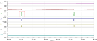
    thank you for your reply. Customer can see the current go across the transistor in the start up situation. In this case, the current must be over 1.5A which is abs rating in an instant. Is it possible to ignore it in this case and what time it can be tolerated? I can get the waveform from customer if you need.

    best regards,

    uchihara 

  • Hello Uchihara, 

    You have sent the schematic from a BOOST converter setup, so I expect that the customer is using the MC33063 as a BOOST.

    Can you please show me in this little schematic that you sent, how a current can go from the input through the transistor into the output capacitor?

    And what exactly do you call the "start up situation"?


    Thanks
    Harry

  • Hi Harry,

    Yes. you are right. It's a boost converter setup. The startup time referes to the period from when the oscillator starts operation at the voltage (3V) until the boost operation stabilize.


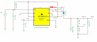
    Sorry for bad resolution. It's a TINA-TI simulation results based on customer schematic. It's same figure in previous my thread as you mentioned.

    Customer can also see such a I_SW in actual board. I hope it's acceptable. If so, please explain the reason even though the datasheet spec is 1.5A abs.

    Best Regards,

    Uchihara

  • Hello Uchihara,

    I am sorry, but we are going in circles here.

    - When the transistor is ON: All current that goes in on pin 1 will come out on pin 2 and go to GND (red path). None of this current will chare the output capacitor.
    - When the transistor is OFF: All current from the inductor will charge the output capacitor. (blue path). No current will fow across the transistor.

    - The current through the transistor is used to "charge" the inductor with energy. The current through the inductor / transistor will ramp up as long as the transistor is turned on.
    - The transistor has to be turned off before this current exceeds 1.5A.

    - The transistor is specified for 1.5A max.
    - 8A or 9A are way too much and can NOT be ignored at any time.

    - The sense resistor has to be set to a value where the current will not exceed these 1.5A.
    - Maybe, if the whole system reacts slow, it will be necessary to use a different value than the calculated one.

    - Looking at the TINA model does not help much. This model is no longer supported, and I cannot know if it delivers plausible results.
    - Please use the PSpice model instead.

    - Did the customer disconnect pin 1 and insert a cable loop to be able to measure that current through the transistor with a current probe?
    - Which maximum current do they measure that way?


    Thanks and regards
    Harry

  • Hi Harry,

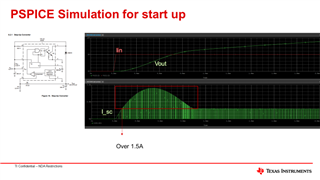
    I simulated the MC33063 and check the start up wave forme for I_sc.

    I used the schematic of the boost topology on the datasheet figure 10. The red squire is the over spec of the I_SC. What do I think this even though our datasheet boost parameter? Is it acceptable ? in this case, please explain the reason.

    Best regards,

    Uchihara

  • Hello Masayuki Uchihara,

    This device is using bipolar transistors so the internal drive current and hFE define the maximum current through the switch. In addition, the device does not stop switching when the peak current is reached (set by the resistor between VIN and IPK), but just increases the charge current for CT.

    Only CT peak voltage turns off the switch. So higher currents than set by the resistor are expected and should not harm the device.

    Best regards,
    Brigitte