This thread has been locked.
If you have a related question, please click the "Ask a related question" button in the top right corner. The newly created question will be automatically linked to this question.
Tool/software:
Dears,
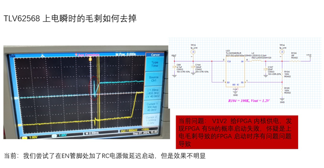
In the previous version of the customer, the FPGA core was powered by LDO. In order to reduce power consumption, the customer now wants to use DCDC: TLV62568 for power supply.
Current problem: Using V1V1 to power the FPGA, it is found that there is a 5% probability that the FPGA will fail to start. It is suspected that the FPGA startup timing is caused by power-on glitches. Please help analyze the cause.
In addition, the customer currently tried to add an RC power supply at the EN pin for delayed startup, but the effect was not obvious.
Hi Arabella,
The schematic looks ok but could you please translate the comments in the picture into English.
Unfortunately, I don't understand the scope plot at all. I think that the blue curve is the output voltage of 1.2V and the yellow curve is the input voltage of 3V, correct?
But why we have an output before the input is supplied?
Best regards,
Sepp
Hi Josef,
The blue one is the 1.2v output voltage (3.3v has a slow start), and both voltage inputs are directly connected to the external power supply (through a PMOS anti-reverse connection circuit, the D of the MOS is connected to the power supply, and the S is connected as the power output). I strongly suspect that the DCDC input capacitor charging just reaches the CE enable threshold, which triggers the DCDC to enter the working state, and then for some reason the DCDC enters the shutdown state again?
(I have described all the Chinese in the picture in English in the original text)
Best Regards,
Arabella
A few additional questions
1. What is the input current of the FB pin of tlv62568? Knowing this value, customers can calculate the feedback resistance and estimate the output voltage more accurately.
2. What is the input current of the FB pin of tlv61070? The input current of the FB pin of tlv61070 is larger than that of Shengbangwei 6603. In some cases, the voltage divider resistor must be modified when replacing each other.
3. The customer originally planned to use tlv62568 to power the FPGA core, but there is a 5% probability that the FPGA will fail to start. Currently, it can only switch back to the LDO power supply solution. If you have a good idea, please give your advice.
Many thanks
Hi Arabella,
In general, this startup behavior of the TLV62568 is not normal. So could you please provide
- a plot were we can see the VIN/EN voltage at this time frame
- the schematic of the application including the power switch and the 3.3V supply because we see a voltage dip also on the 3.3V output which has nothing to do with the 1.2V.
In the meantime I will check your additional questions.
Best regards,
Sepp
A few additional questions
1. What is the input current of the FB pin of tlv62568? Knowing this value, customers can calculate the feedback resistance and estimate the output voltage more accurately.
2. What is the input current of the FB pin of tlv61070? The input current of the FB pin of tlv61070 is larger than that of Shengbangwei 6603. In some cases, the voltage divider resistor must be modified when replacing each other.
3. The customer originally planned to use tlv62568 to power the FPGA core, but there is a 5% probability that the FPGA will fail to start. Currently, it can only switch back to the LDO power supply solution. If you have a good idea, please give your advice.
Hi Arabella,
Could you please provide the plots I have requested 2 weeks ago to solve the startup issue.
Best regards,
Sepp