


Tool/software:
Hello,
On BQ76952, certain protections can be configured to disable both CHG and DSG FETs, but not all of them -
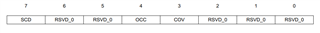

Is there a reason for the chip not to allow both CHG and DSG FETs to open when a fault occurs? In other words, do RSVD bits in these registers really have no meaning? The layout of bits in these registers looks like the original intention was to provide that flexibility, but then it was changed.
Also, this statement:
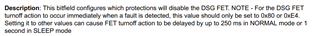
- does it mean that if I, for example, disable OCD2 FET action in "DSG FET Protections A", I will incur extra delay?
- does the extra delay affect FET action, or ALERT pin timing as well?
Thank you!
