This thread has been locked.

If you have a related question, please click the "Ask a related question" button in the top right corner. The newly created question will be automatically linked to this question.

LMZ35003: Design Check: +48Vin -> 5V, 12Vout

Part Number: LMZ35003

Tool/software:

I am building a power supply board which will use the LMZ35033 to generate 5V, 12V from +48V. Any feedback is appreciated.

Design

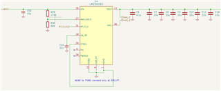
  • The only difference between the two configs is the Vset resistor (53.6K, 140K)
  • and the RT clock resistor (1.1M, 267K) per the recommendations.
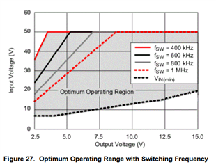
  • Divider for UVLO chosen for '40.0V (~83% of nominal input)

Questions/comments

1) I do not need PWRGD functionality. Can i leave it floating, or should I ground it? The datasheet says "a pull up resistor is required" but perhaps it is only means "is required if you want to use it"

2) I have a TVS on the input (not shown, SMAJ48A-13-F) to protect against transients on startup. Is this a good choice, or is there something better?

3) Output capacitance: I have 6x 22 uF (132 uF). These (C3225X7R1C226M250AC) retain 84 uF even at 12V bias. The ones in the EVM do not obey the guidelines in the datasheet. First, in that its only 88 uF at 0V bias, and also by 12V bias the output capacitance drops to 26 uF.

  • Hello Adam,

    I would suggest you design around 5Vout and operate at 1MHz. Selecting 1MHz and the associated cap to stabilize the 5V design (~100uF) should also result in a stable design when you dynamically change the VSET resistor to change the output voltage to 12V, while enabling the device to support load currents up to 2.5A.

    1. PWRGD if not used can be left floating.

    2.  I haven't looked to closely at 50V TVS', but, for our 36V devices, I see most customers using a 33V (nom) TVS to allow for the max clamp voltage to still fall below the absmax on vin. I think you are on the right track with your selection.

    3. The output capacitance derating you determined seems adequate for the design.

    Looks like the EVM is using 25V ceramics and a bulk electrolytic. It maybe on the low side for our recommendation at higher output voltages. Our recommendation maybe a bit on the conservative side, as in-general, with fixed int comp CM bucks, at higher output voltages, the dominant load pole (output cap) doesn't  need to be as low in frequency to stabilize the loop.

  • Hi Marshall ,

    Thank you very much for your very comprehensive answer!

    I may have been unclear on one point. The board will have two LMZ35003, one for 5V, one for 12V I don't need to change dynamically.

    I wasn't sure how to interpret Figure 27, but I set the frequency lower for the 5 V because I thought the guidance on pg 16 implied with 48Vin and 5V out i would have to  operate at <600 kHz to avoid huge amount of pulse skipping or maybe stability issues, though to be honest I am not sure how to interpret 'optimum operating region'.

  • Hi Adam,

    You are welcome.

    Thank you for clarifying.

    That figure could use some clarification :) 

    The switching frequency series shows as vout decreases (going right to left on the x-axis) the input voltage must fall to continue to operate at a constant frequency. The device has a minimum on-time (min duty cycle) for the high-side current sense blanking time.

    For example with your 5V design, if you want to operate at 400kHz, at 48Vin, you must operate at 400kHz or lower. If you program the device for a higher switching frequency the device will still be in regulation, but the frequency will be reduced and on-time will be at its minimum. The device does this automatically.

    The vin min series is a bit confusing to me. There is a minimum off time associate with a NMOS buck to refresh the boot cap charge, but, that would be related to the switching frequency and there is only one series. The device does has dropout voltage which is related to the max duty, RDS of high side, DCR of inductor and loading. I suppose the curve is speaking to the dropout voltage (VIN to VOUT differential needed) at max load current, but, it seems excessive to me.

  • OK thank you for the further details.

    I was copying figure 30 in my selection of the clock for the 5V out configuration. But based on what you are saying I may as well leave it at 400 kHz given my input voltage. The 12V I will leave as-is.

    Thanks again.

  • Sounds good. You are welcome