This thread has been locked.

If you have a related question, please click the "Ask a related question" button in the top right corner. The newly created question will be automatically linked to this question.

TPS546D24A: TPS546D24A output abnormal

Part Number: TPS546D24A
Other Parts Discussed in Thread: TPS546D24

Tool/software:

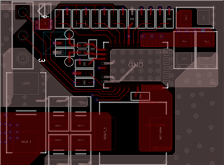
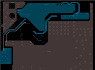
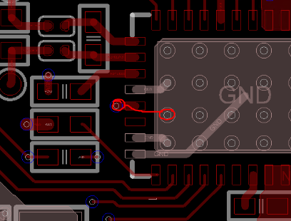
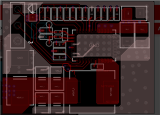
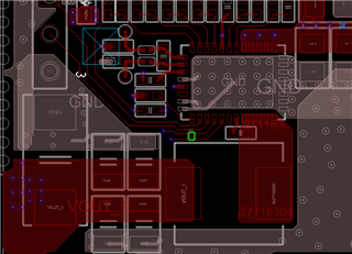
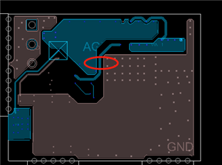
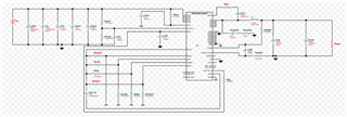
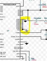
I made a DC-DC module using TPS546D24A,the sch is as follows

SCH

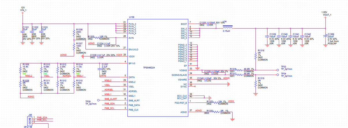
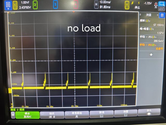
But the output is abnormal.When there is no load,the output is strange

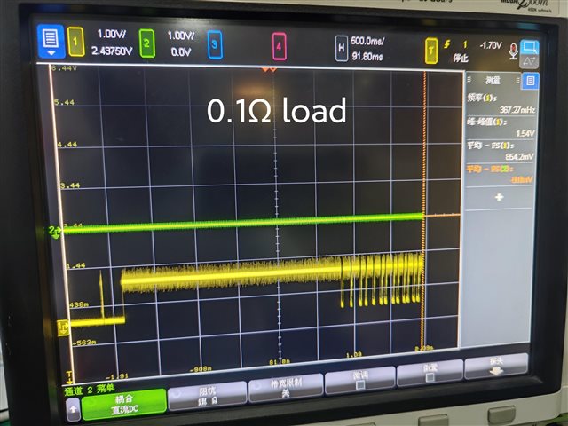
And when the load is a 0.1Ω resistor,it can work normally for few seconds but become abnormal soon.

I wonder is there any mistakes in the schematic? And the possible reason for this phenomenon

  • I see the schematic shows TPS546D24, but the post mentions TPS546D24A. Which one are you using? They have different pin strap values.

    Thanks!
    Tomoya

  • I use TPS546D24A

  • Hi,

    Thank you for your clarification. I reviewed the schematic, and nothing stands out as a major concern. You might want to try a more aggressive loop compensation by using COMP code 8 instead of code 7. To do this, change R1315 from 4.64k to 5.62k. If this adjustment does not lead to any improvements, I suspect there may be an issue with the layout, a part of the schematic that hasn’t been shown, or possibly with the setup itself.

    Could you please share the layout with me? I would be happy to review it as well. Additionally, if you have PMBus communication, could you check the status register to see which fault or warning was triggered by the device?

    Thank you,
    Tomoya.

  • Hi,

    I have one more thing to add. Are you using PMBus to configure a non-default setup? If so, please share the details. If you're using the TI FUSION GUI, please provide either the project file or the text file.

    Thank you,
    Tomoya

  • Hi

    I haven't use pmbus yet.And I changed R1315 to 5.62k but the results is still same as before.

    It is a small module to verify output function,so all the schematic has been shown.The layout is as follows,


  • Hello,

    The current layout does not include a direct connection between AGND and PGND at the thermal pad, as recommended in the datasheet. This may be contributing to false overcurrent (OC) detection and subsequent shutdowns or restarts due to issues with current sensing. To investigate this, please connect the via on the thermal pad to a via on the back side and check if the problem improves. Additionally, it might be beneficial to remove R1330 at the same time.

    Thank you,
    Tomoya

  • Hello,

    I noticed something else with the layout. The BP1V5 bypass capacitor isn't positioned close to the device, and this can lead to performance issues with the regulator. Would it be possible to add a 2.2µF capacitor right at the pins of BP1V5 and DRTN? This might help resolve the issue. 

    Thank you,
    Tomoya

  • I add a 2.2uF cap between BP1V5 and DRTN at the position of green rectangle,but there is no changement. 

    And I try to  a 0R at bottom of GND and AGND,the output become difference as before,so maybe the reason of output abnormal is the connection of AGND and GND.

    But I still have a question, the typical application shows that GND and AGND should be separated,how can I deal with them in layout?

  • Hello,

    The Webench schematic shows that AGND connects to PGND. I apologize if this was unclear.

    The layout follows the pin description in the datasheet, which states that you should connect the AGND pin directly to the thermal pad.

    In the schematic, we show this connection in the application circuit from the datasheet. We use a "Net-Tie," which is a metal trace that connects the AGND net to the GND net on the PCB layout.

    Thank you,
    Tomoya