Because of the Thanksgiving holiday in the U.S., TI E2E™ design support forum responses may be delayed from November 25 through December 2. Thank you for your patience.

UCD3138FW-BIDI: Support setting cbc

Part Number: UCD3138FW-BIDI
Other Parts Discussed in Thread: TIDA-00653,

Tool/software:

Dear TI Experts,

Reference project: TIDA-00653、UCD3138FW-BIDI

We plan to use the TIDA-00653 as a reference circuit and add PCM functionality. However, I found that PCM is controlled by the EADC, and since the TIDA-00653 circuit has four-phase current, it seems that using EADC's PCM for each phase is not feasible.

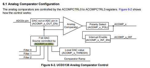
Currently, we are focusing on CBC. I found that the comparator source for CBC can select a filter as the source. If "ACOMP_x_SEL" selects the filter as the source, does the filter need any specific configuration? Where can we view the corresponding values for the filter source?

Alternatively, do you have other recommendations for PCM control that could be applied to four-phase current?
To simply test and verify the configuration EADC0 -> Filter0 -> CBC -> DPWM1, how should I set it up?

Below is my configuration. Is there any issue with these settings? After I completed the setup and enabled the CBC function, DPWMA remains in a fully LOW state. Neither controlling EADC’s EAP0 nor adjusting the DAC_Value produces any change.

void eadc_filter_cbc()
{
    /* dpwm 1 */
    Dpwm1Regs.DPWMCTRL0.bit.PWM_EN = 0;   //disable locally for init
    Dpwm1Regs.DPWMCTRL0.bit.CLA_EN = 0;     //default is 1 - use cla

    Dpwm1Regs.DPWMCTRL0.bit.PWM_MODE = 0; //normal mode
    Dpwm1Regs.DPWMPRD.all = DPWM_PERIOD; //use .all for all values, make sure scaling matches.
    Dpwm1Regs.DPWMEV1.all = (DEAD_TIME_1) + 10; //Put event 1 at start of period
    Dpwm1Regs.DPWMEV2.all = ((DPWM_PERIOD) >> 1) - (DEAD_TIME_2) / 2; //1/4 of period - divide is OK because it's all constants.
    Dpwm1Regs.DPWMEV3.all = ((DPWM_PERIOD) >> 1) + (DEAD_TIME_2) / 2;       //1/2 of period
    Dpwm1Regs.DPWMEV4.all = 10;
    Dpwm1Regs.DPWMSAMPTRIG1.all = 2000;

    Dpwm1Regs.DPWMMINDUTYHI.all = 2250;
    Dpwm1Regs.DPWMMINDUTYLO.all = 2250;

    Dpwm1Regs.DPWMCTRL0.bit.MIN_DUTY_MODE = 2;
    Dpwm1Regs.DPWMCTRL0.bit.PWM_EN = 1;     //enable locally

    /* filter 0 */
    Filter0Regs.FILTERKPCOEF0.bit.KP_COEF_0 = 1;
    Filter0Regs.FILTERKICOEF0.bit.KI_COEF_0 = 0;
    Filter0Regs.FILTERKDCOEF0.bit.KD_COEF_0 = 0;
    Filter0Regs.FILTERKDALPHA.bit.KD_ALPHA_0 = 0;

    Filter0Regs.FILTERKICLPHI.bit.KI_CLAMP_HIGH = 0x7FFFFF;
    Filter0Regs.FILTERKICLPLO.bit.KI_CLAMP_LOW = 0;

    Filter0Regs.FILTEROCLPHI.bit.OUTPUT_CLAMP_HIGH = 0x7FFFFF;
    Filter0Regs.FILTEROCLPLO.bit.OUTPUT_CLAMP_LOW = 0;

    Filter0Regs.FILTERCTRL.bit.FILTER_EN = 1;
    // enable OK here, because nothing will happen until DPWM and front end are globally enabled

    // Better option for handling shoot through - uses full dynamic range of filter
    Filter0Regs.FILTERCTRL.bit.OUTPUT_MULT_SEL = 1;         // select half period kcomp for output multiplier

    /* loop mux */
//    LoopMuxRegs.DPWMMUX.bit.DPWM0_FILTER_SEL = 0; // use filter 0 for DPWM 1
    LoopMuxRegs.SAMPTRIGCTRL.bit.FE0_TRIG_DPWM1_EN = 1; // use DPWM1 for filter0 sample trigger
    LoopMuxRegs.FILTERMUX.bit.FILTER0_FE_SEL = 0; // connect filter 0 to front end 0.
    LoopMuxRegs.FILTERMUX.bit.FILTER0_PER_SEL = 1; // Selects source of switching cycle period for Filter 0 Module

    /* eadc */
    FeCtrl0Regs.EADCDAC.bit.DAC_VALUE = 8192;
    FeCtrl0Regs.EADCCTRL.bit.AFE_GAIN = 2;

    /* global */
    union GLBEN_REG glben_store; // collect global enable bits for simultaneous use
    glben_store.all = 0;
    glben_store.bit.DPWM1_EN = 1;
    glben_store.bit.FE_CTRL0_EN = 1;
    LoopMuxRegs.GLBEN = glben_store;
	
	
	/* cbc - dpwm1 */
    //Phase 1 CBC
    FaultMuxRegs.ACOMPCTRL0.bit.ACOMP_B_SEL = 2; // 2 = Analog Comparator B Threshold set by Filter 0 Output
    FaultMuxRegs.ACOMPCTRL0.bit.ACOMP_B_POL = 1; // 1 = Comparator result enabled when input exceeds threshold (Default)
    FaultMuxRegs.ACOMPCTRL0.bit.ACOMP_EN = 1; //1 = Analog Comparators Enabled
    FaultMuxRegs.DPWM1CLIM.bit.ACOMP_B_EN = 1; //AD03 //1 = Analog Comparator result enabled for current limit

    Dpwm1Regs.DPWMCTRL0.bit.CBC_ADV_CNT_EN = 1; //1 = CBC enabled (pwm mode: normal mode)
    Dpwm1Regs.DPWMCTRL0.bit.CBC_PWM_AB_EN = 1; //1 = PWM-A and PWM-B affected by Fault CBC
}

  • Hi Parrish,

    Your query is under review.

    I will get back to you in a day.


    Regards
    Hemanth

  • Hi Parrish,

    Your configuration looks ok except for the configured Kp value. You have given Kp=1 which is very low to generate any significant duty value by the filter and because of this CBC will go high even before the EVENT1, this is the reason for DPWMA remains low throughout the period. You can try configuring Kp= 0x7fff (Pass through the error value as it is, in other words multiplicand is 1; for lower values use a value lower than 0x7fff). This should help you in solving the issue.


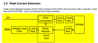
    Regarding using analog comparator for PCM, it is recommended to use PCM module in front end for the PCM control. The most significant problem you may face with analog comparator is in ramp generation. For a stable operation in PCM with duty cycle higher than 50% you require negative slope compensation which is implemented using ramp generator.

    The ramp resolution depends on the DACs. In front end, the DAC is of 10 bit which has a 1.5mV resolution without dithering and 0.1mV resolution with dithering whereas the analog comparator DAC is of 7 bit with a resolution of 20mV. This lower resolution of analog comparator DAC can cause issues with slope compensation and stability.

    Regards

    Hemanth

  • Dear Hemanth,

    Based on your suggestion, I modified the kp value (kp = 10000 or kp = 0x7fff), but DPWMA still remains at a low voltage. Currently, EAP0 is providing 0.5V, and adjusting the voltage of EAP0 or DAC_VALUE also has no effect.

    Could you advise which register content I can refer to for the 7-bit DAC in the filter output to ACOMP_x_SEL?


    Additionally, we initially considered using EADC for PCM. However, since our current circuit is an extension based on TIDA-00653, using PCM for each phase's current might not work directly with EADC. Is this the reason why the original program design lacks any PCM-related content?

    So, for now, we’ll try to route the "voltage loop filter" of vout to the CBC to achieve current limiting.

  • Parrish,

    When you modified the Kp value, what was the input applied to comparator input terminal? Was it left floating?

    When we tried with floating input, the behavior is as mentioned by you. However, when the comparator input is connected to a signal, it behaves correctly. If you don't have a signal to connect, connect the terminal to ground instead of leaving it floating. Please confirm.

    There are only total three front ends and only one EADC can be used for PCMC. So, in TIDA-00653, PCM was not available.

    Can you please clarify on this - "Could you advise which register content I can refer to for the 7-bit DAC in the filter output to ACOMP_x_SEL?". Do you want to read the content of 7-bit DAC of comparator? If yes, I don't know of a way to read back the content again from DAC. The MUX ACOMP_x_SEL itself decides what is the source for the DAC input.

    Regards

    Hemanth

  • Dear Hemanth,

    I'm using a signal generator to produce a 100kHz sawtooth wave to simulate the input at the ADC pin, and the DPWM frequency is also set to 100kHz.

    Yes, I’d like to understand what kind of content is being carried by the source that ACOMP_x_SEL compares with the ADC when ACOMP_x_SEL is set to the filter. It mentions a "7-bit DAC" (similar to how I can use ACOMP_x_THRESH to set the limit voltage). Alternatively, can I calculate this from the value of FILTERYNREAD?

  • Parrish,

    Have you synchronized the 100kHz sawtooth signal with PWM?

    Otherwise, connect DPWM0B to AD03 to create a CBC. An example:

    void init_dpwm0(void)
    {
    Dpwm0Regs.DPWMCTRL0.bit.PWM_EN = 0; // disable DPWM1 locally during initilization
    Dpwm0Regs.DPWMCTRL0.bit.CLA_EN = 0;
    Dpwm0Regs.DPWMCTRL0.bit.PWM_MODE = 0;
    Dpwm0Regs.DPWMPRD.all = DPWM_PERIOD;
    Dpwm0Regs.DPWMEV1.all = 0;
    Dpwm0Regs.DPWMEV2.all = 10000;
    Dpwm0Regs.DPWMEV3.all = 12000;
    Dpwm0Regs.DPWMEV4.all = 18000;
    Dpwm0Regs.DPWMCTRL0.bit.MSYNC_SLAVE_EN = 1;
    Dpwm0Regs.DPWMPHASETRIG.all = 0;
    LoopMuxRegs.DPWMMUX.bit.DPWM0_SYNC_SEL = 1;

    Dpwm0Regs.DPWMCTRL0.bit.PWM_EN = 1; // enable DPWM0 locally
    LoopMuxRegs.GLBEN.bit.DPWM0_EN = 1; // enable DPWM0 globally
    }

    Refer ACOMPTCTRLx registers to configure the analog comparator thresholds.

    A snippet from TRM.

    Regards

    Hemanth

  • Dear Hemanth,

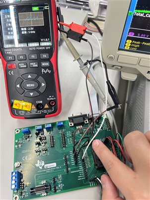
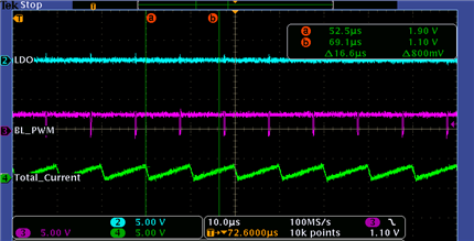
    I am using an external signal generator to simulate a sawtooth signal, connecting the signal to AD03.

    As shown in the figure:

    2: DPWM1 A,
    3: DPWM1 B,
    4: Sawtooth signal (100kHz)

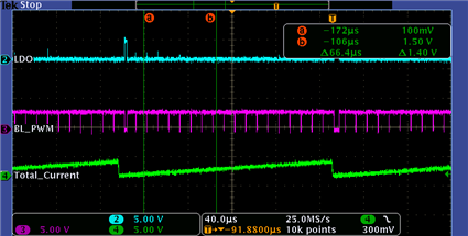
    As shown in the figure:

    2: DPWM1 A,
    3: DPWM1 B,
    4: Sawtooth signal (5kHz)

    I don't quite understand why connect DPWM0B to AD03. Isn’t the ADC input voltage range 0~2.5V?

  • Hi Parresh,

    I recommended DPWM0B to connect to AD03 (may be via RC filter) to generate inherently synchronized ramp signal.

    Regards

    Hemanth