This thread has been locked.

If you have a related question, please click the "Ask a related question" button in the top right corner. The newly created question will be automatically linked to this question.

UCC28951-Q1: PSFB using SiC MOSFETs

Part Number: UCC28951-Q1
Other Parts Discussed in Thread: UCC28951

Tool/software:

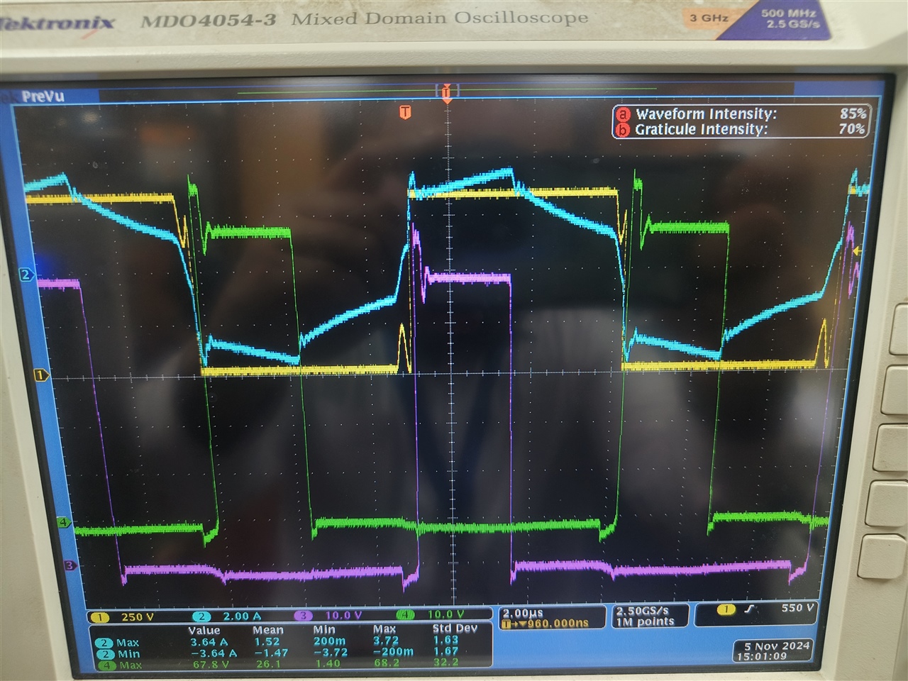
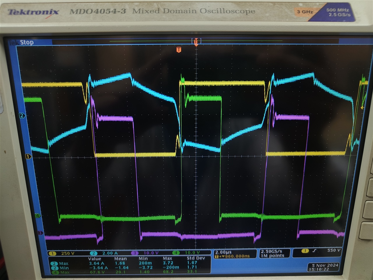
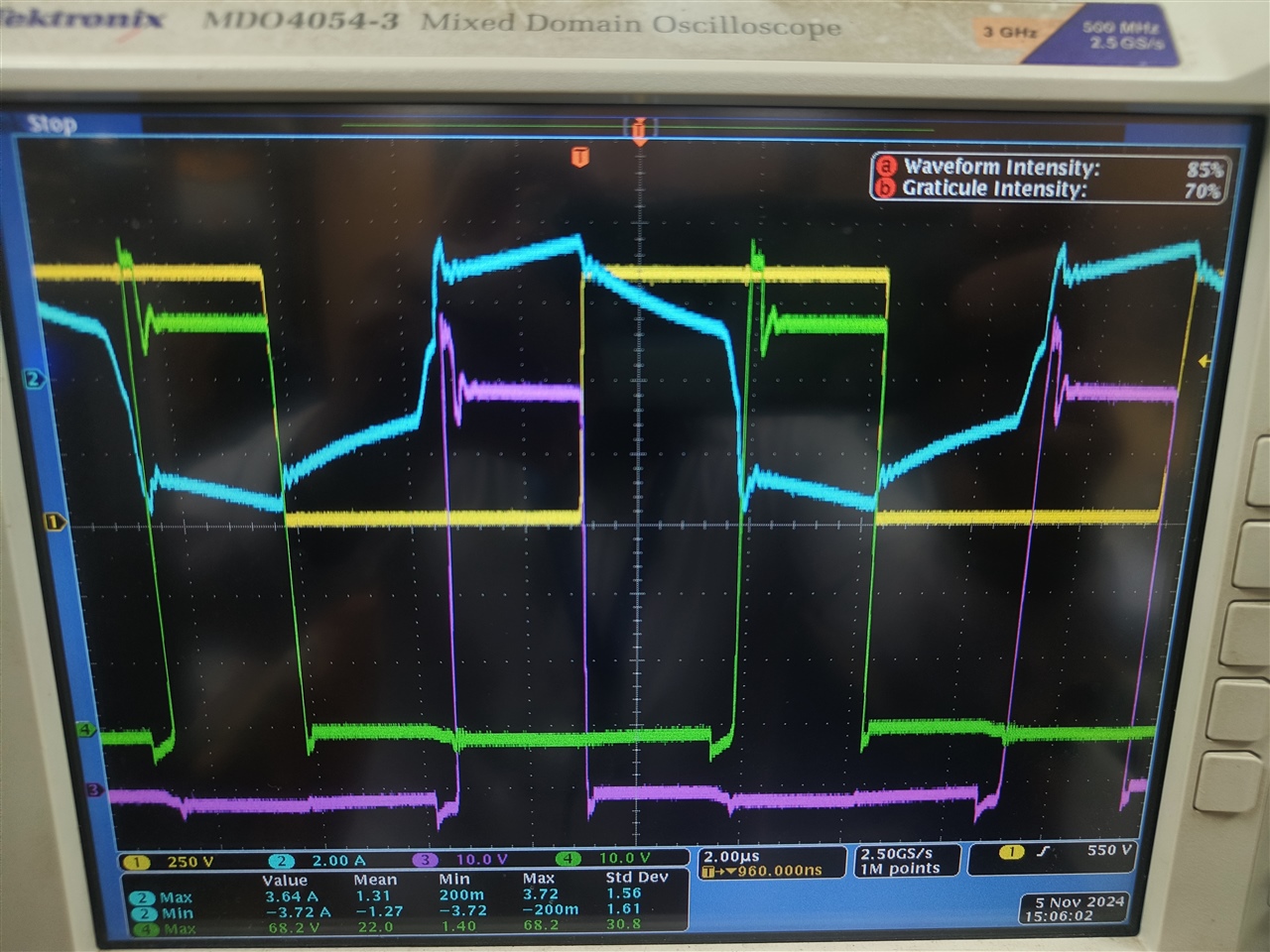
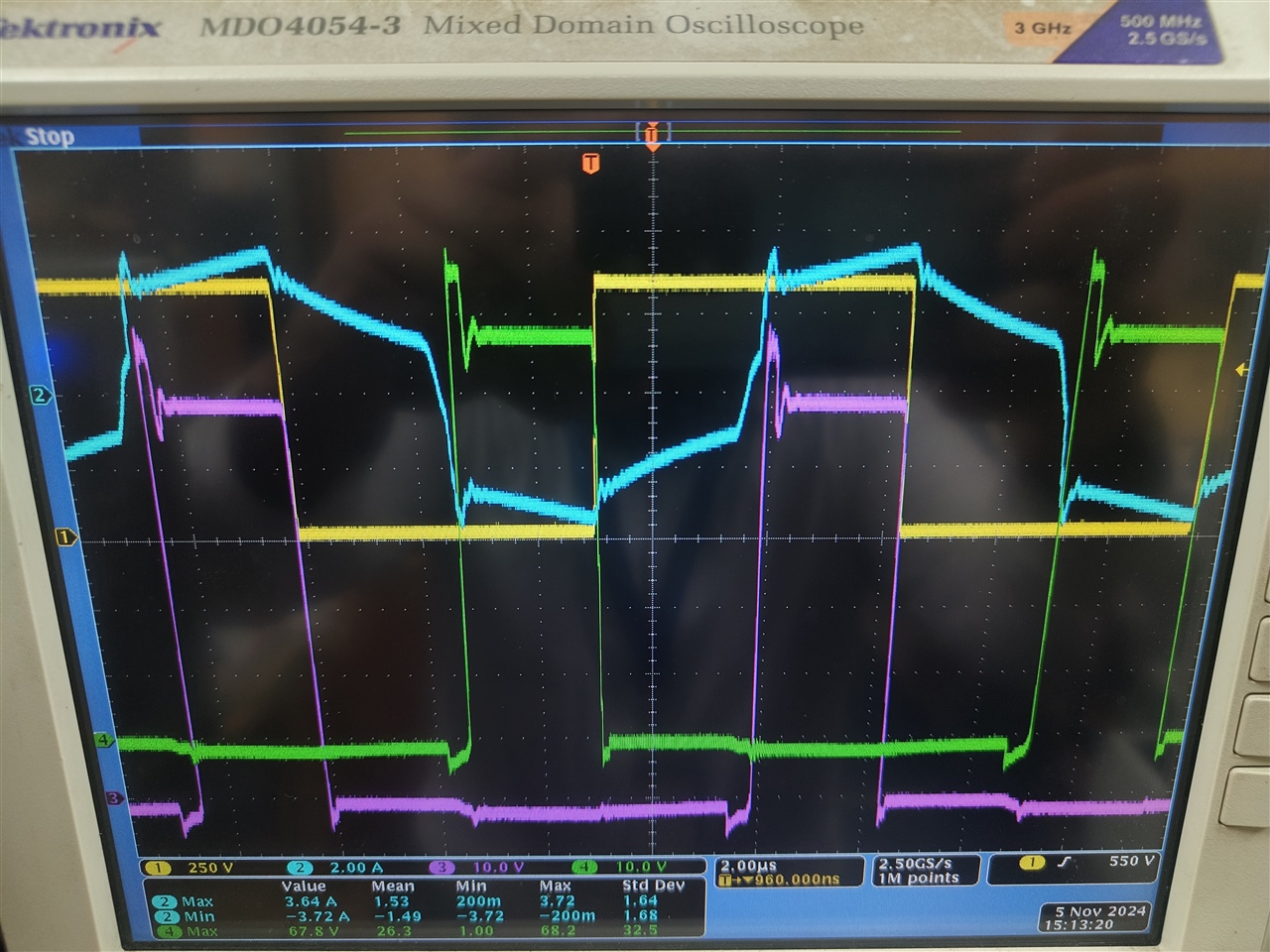
Testing using SiC MOSFETs 

Scenario: Vin:810VDC, load : 43Adc

Below are gate drain source of primary MOSFETs. Resonant inductor is not being used. Transformer leakage inductance: 22uH, turns ratio : 27, output voltage: 23.5VDC. DCM pin is connected to ground. CS filter : 1K, 1nF. Fixed delay approach. Adaptive delay is grounded. 

Blue : primary current 

Purple: synchronous FET F

Green : synchronous FET E

Yellow: A drain source 

Yellow: B drain source 

Yellow: C drain source

Yellow: D drain source

1. C and D drain source waveform looks proper square wave, why not A and B ?

2. I'm Operating synchronous FETs now in CCM mode. I understand DELEF delay resistor might be little off for now, that I will try to adjust.Earlier Even in diode mode I had leading edge current spike issue. How to troubleshoot or remove this ? 

3. As per excel calculation, the transformer ring might disappear of I reduce  DELAB DELCD values. But if I add Shim. Inductor, the DELAB DELCD values are increasing. Is it ok ?

4. What more can be done to improve this design? Kindly assist. 

  • Hello,

    Your schematic is under review and I will get back to you shortly.

    Regards,

  • Hello,

    1. C and D drain source waveform looks proper square wave, why not A and B ?

    > Your QDd switch nodes timing is setup to ZVS, this is why QD drain to source and QC drain to source look like square waves.

    > Your Ls and Llk does not have enough energy stored to achieve ZVS QBd to achieve ZVS also your turn-on delay is not setup correctly.  This is why you see ringing and not a square waves across FETs QA and QB drain to source.

           * You need to setup the turn-on delay to 1/4 the tank frequency of (Llk +Ls) and the switch node capacitance.

           * If you want to achieve ZVS at this power level you need to increase the size of Ls.

           * The following link will bring you to an application not that goes through detail on how size Ls and setup the turn on delays of FETs QA through QD to                  achieve ZVS/valley switching.  https://www.ti.com/lit/pdf/slua560

    2. I'm Operating synchronous FETs now in CCM mode. I understand DELEF delay resistor might be little off for now, that I will try to adjust.Earlier Even in diode mode I had leading edge current spike issue. How to troubleshoot or remove this ? 

    > Leading edge current spike is typical when driving FETs.  The only issues is when it comes to current sensing.  You should be able to filter this out with low pass RC filter.  1k and 220 pF from the current sense resistor to the CS pin of the UCC28951 should do the trick.

    3. As per excel calculation, the transformer ring might disappear of I reduce  DELAB DELCD values. But if I add Shim. Inductor, the DELAB DELCD values are increasing. Is it ok ?

    >You are correct that reducing the QA and QB turn-on delays will reduce the ringing.

    >Increasing Ls will provide more energy for ZVS.  Please note that will change the resonant ring.  You might want to increase the shim inductor first before resetting the timing.  

    4. What more can be done to improve this design? Kindly assist. 

    >I do think the things recommend above will improve the voltage across FETs QA and QB.

    >If you followed the excel tool on QBd you will get ZVS down to 50% load.  Increasing Ls will allow QBd to obtain ZVS down to lighter loads.

    Thank you for interest in Texas Instruments (TI) products.  If you have a related question, please click the "Ask a related question" button in the top right corner. The newly created question will be automatically linked to this question.

    Regards,