This thread has been locked.

If you have a related question, please click the "Ask a related question" button in the top right corner. The newly created question will be automatically linked to this question.

TPS548B22: Thermal calculator and model

Part Number: TPS548B22

Tool/software:

Hi Expert,

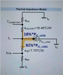
Is there a calculator to help estimate thermal? Also, is there a thermal model that would let us know what percentage of heat is dissipated through the PCB and how much is dissipated through the case?

Regards,
Hailiang

  • Hi Expert,

    Here is a competitor's model for your reference. 

    Regards,
    Hailiang

  •  

    The thermal information is provided in the datasheet is section 6.4 (currently on page 5) https://www.ti.com/lit/ds/symlink/tps548b22.pdf#page=5 

    Θjc(top) is 18.3 °C/W

    Θjc(bottom) is 0.6 °C/W

    Ψjc(top) which is the "Characterization parameter" for measuring the die temperature based on the top-side case temperature and the total IC output power is 0.96°C/W

    You can calculate the percentage of IC power flowing through the top and bottom by the ratio of Ψjc(top) / Θjc(top) ≈ 5% 

    With Natural Convection, the Θca(top) of a 5mm x 7mm QFN is >200 °C/W do to the small surface area and constricted airflow

    And important note:  Ψjc(top) and the percentage of power dissipated in each path is heavily dependent on the total PCB thermal resistance Θba which depends on the PCB construction and layout, particularly the ground plane and its connection to the exposed pad on the backside of the TPS548B22.

    The JEDEC reference design board, which is a 75mm x 75mm, 4-layer, 0.5oz copper / layer layout with pin-width traces from each pin to the perimeter of the board and no connection from the exposed pad to the internal layers has a Θba of 24.9 °C/W for a total junction to ambient thermal resistance of 28.5 °C/W and 95% of the heat flowing into the PCB.

    Our EVM, which is a 6-layer, 2oz copper per layer (though 1 layer is only used for signal routing)  has a Θba of about 12 °C/W and more than 95% of the IC power dissipation flows through the exposed pad and into the PCB.

    For an estimation of the power dissipation of the TPS548B22, I would recommend using WeBench Power Designer - https://www.ti.com/product/TPS548B22#design-development 

  • Hi Peter,

    I want to know why the ratio of ΨJT to ΘJC(top) represents the proportion of dissipation from the top case? Is it because ΘJC(top) represents the thermal resistance when dissipating heat from the Top case alone, while ΨJT represents the thermal resistance of the top case when it naturally uses multiple paths to dissipate heat without special control? Is this understanding correct?

    Regards,
    Hailiang

  • I want to know why the ratio of ΨJT to ΘJC(top) represents the proportion of dissipation from the top case? Is it because ΘJC(top) represents the thermal resistance when dissipating heat from the Top case alone, while ΨJT represents the thermal resistance of the top case when it naturally uses multiple paths to dissipate heat without special control?

     ΘJC(top) is the actual thermal resistance of heat flowing from the die surface (junction) to the top of the package.

    ΨJT(top) is the temperature rise from the die surface (junction) to the top of the case divided by the total IC power dissipation, Pdiss(ic)

    Since the rise from Junction to Top is ΘJC(top) x Pdiss(ic) x %top

    and 

    Rise from Junction to Top is also equal to ΨJT(top) x Pdiss(ic)

    We Get:

     ΘJC(top) x Pdiss(ic) x %top = ΨJT(top) x Pdiss(ic) 

    Pdiss(ic) drops from both sides and we have:

     ΘJC(top) x %top = ΨJT(top)

    %top = ΨJT(top) / ΘJC(top)