Because of the Thanksgiving holiday in the U.S., TI E2E™ design support forum responses may be delayed from November 25 through December 2. Thank you for your patience.

UCC25660: UCC256601 FB questions

Part Number: UCC25660
Other Parts Discussed in Thread: ISOM8110, LM431

Tool/software:

Hi,

When it comes to the UCC256601 LLC controller i need isolated FB , this is normally done through an optocoupler but i noticed that TI has some optoemulators available.

I was wandering how to design to use them. Also i am not sure how to set the mirrored FB current properly and how it should scale through the optocoupler/optoemulator.

THX in advance

  • Hello Dietrich, 

    Thank you for your interest in our opto-emulators! Opto-emulators are designed to be p2p and functionally equivalent to traditional optocouplers. You can find a lot of app notes with the benefits of upgrading to a non-light based isolation solution in the ISOM8110 product page. Also, please see PMP23470 reference design | TI.com which showcases ISOM8110 in the feedback loop of a flyback converter. 

    I would like to point out that ISOM8110 does have a minimum IF of 700uA. Below this range the diode emulator will not be on, and no signal will be transmitted. This can be an issue for newer controllers where the FB current is very small. 

    Let me know what questions you have. 

    Best,
    Andrew

  • Dear Andrew,

    THX for your super fast responce, here is a list of questions:

    1 from i read optoemulators are with better bandwidth and are sort of a direct replacement but I never used optocoupler before in analogue* mode so i am VERY stuck regarding how to even begin + there seem to be multiple way to do it , can you suggest some resources please?

    2 Regarding reference designs there is the flyback you mentioned , and this reference for my LLC https://www.ti.com/lit/df/tidmd32/tidmd32.pdf?ts=1725389392696  this one has a lot more features like over current

    this: https://www.ti.com/lit/ug/sluucv2a/sluucv2a.pdf?ts=1725333423957&ref_url=https%253A%252F%252Fwww.ti.com%252Ftool%252FUCC25660EVM-064  seems to be closer to what you proposed but i am still not sure how to approach the problem . Or rather said i can copy the schematic, that is easy BUT deciding on part values and understanding the trade offs and the WHY is the problem for me atm. Can you please enlighten me a bit?

    3 i saw most TI designs you a shunt* type voltage reference but i also remember some designs that use opamps a lot of other circuitry to add extra functions ( like the first link i posted) is there any TI guide / resource that explains the how?

    NOTE: my input is from APFC and output is  10Amax 24V* ( after rectification  )

  • Hello Dietrich,

    Correct, opto-emulators will have a faster bandwidth and have better isolation performance over lifetime due. See Replacing Optocouplers With Opto-Emulators for more details.  Unfortunately, UCC25660x will not be compatible with the ISOM8110. The UCCx device requires a very low current on the feedback pin which the ISOM8110 cannot provide (minimum forward current of 700uA). However, for most optocoupler applications ISOM8110 will be drop in replace. 

    For the general flyback controller questions, I will have to pass this thread along to a different team. If you have more questions about Isolation devices like opt-emulators feel free to make another thread.

    Best,
    Andrew

  • THX

    So then if optoisolators are not going to work with UCC25660x.Then How would i design a optocoupler FB for my circuit?

    I also plan to have a Hall effect sensor for over current protection ( i am also open to other types like shunt + INA IC and other).

    There is not guide on the UCC25660x datasheet on how to do isolated FB so i came here to ask .....

  • Hi Dietrick,

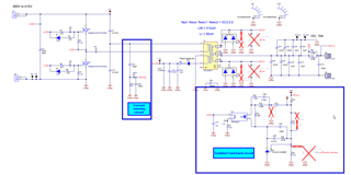
    Please use the opto coupler based isolated feedback which is shown in the data sheet and the EVM user guide: https://www.ti.com/lit/pdf/sluucv2

    For over current protection, you can use the RC differentiator as shown the EVM schematic.

    Let me know if you know if you have any further questions.

    Regards

    Manikanta P 

  • HI,

    So after i studied the FB from the provided circuitry here is what i came up with:

    1 The FB is some sort of current type. On the primary the voltage on the FB pin will be 1.5V IF all current goes to the opto, else it will go through internal 100k and that will be about 8V on the FB pin. I dont really understand how we ended up with 10k as the opto emitter resistor but ill take it as is, ( it should also work as collector resistor from what i see)

    2 on the secondary i understand the R19 R23 are in a divider and they set the ref pin to 1.24V so then the TLVH431ACDBZR acts like some sort of regulated zener that has a 1.24V drop

    3 What is the role of R16 ? Is it some sort of tuning resistor or compensation? since i can see that it steals some current from the opto diode But i dont understand why I would want that and not simply increase R18 or R17 ? Yea voltage over R16 is the same as in the diode so current should be same? If yes then opto diode current is about 1mA

    4* OR is R16 there in order to provide some extra current for the TLVH431ACDBZR since for some reason the current through the opto diode is not enough ? or you want to make sure you have enough regardless of opto diode current?

    4 Assuming opto diode current is 1mA then opto nps current is 1* 1-1.5 from the opto gain BUT that would make the primary permanently fully on so FB pin is at 1.5V the problem is that this happens if Vout on secondary is 12V or more so there is something very wrong with this understanding of FB so please explain.

    5 All capacitors on the FB i know they are for compensation and filtering but i dont understand how you got those values

    Also when first starting a prototype co i need them all from the beginning or can i add and tune them as I go ?

  • Hi Dietrich,

    Lets have a webex meeting to discuss your questions. Could you share your email ID so that I can send a meeting invite?

    Regards

    Manikanta P

  • As of now there is something way more important that needs to be finished by the end of November.

    Hopefully it will be done this week or next week and then after we can talk.

    Also i read a design reference from a xx431 ( 2.5V version, something older with a to-92 part number , old TI reference anyway)  reference and it explained a lot better some stuff and it untangled a few questions.

    Ill return here after the urgent stuff is done, hopefully with a rough draft and some SPICE simulation to help, or worst case more confused.

    Best regards, and sorry again to leave u like this for no but some stuff has changed priority .

  • Hi Pallantla,

    Sorry for the interrupt in the thread but something really needed full attention.

    Meanwhile i also did a bit of reading from some older 2.5V references and i think i understand how it should work.

    So ill return here with that i devised from all my research and then see how good bad it is.

    Hopefully i figured it out correctly  but it can also be a bit off.

    Ill post my schematics with values in here.

    THX in advance.

  • Hi Pallantla,

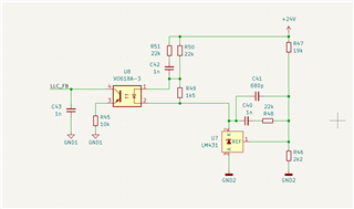
    Here is what i came up after a lot of study.

    I used the same opto coupler so there is no gain complication, 

    R45 - same as in reference design,  C43 is 1n for now mostly as placeholder, i know it is for stability but not sure why 3nF was used initially( probably some low pass filter).

    On the secondary:

    2V5 reference, since i am already using it in my design

    R46 R47 set the FB to slightly over 24V , they were calculated so that 1mA+ flows through this pah since LM431 needs a few uA input in the reference pin ( values subject to change, tho i am sort of convinced that i can get away with X10 current values but used 1mA+ for now since this is not a problem as of now)

    R48 R51 C42 C41 C40 are for some type of pole compensation - not sure how they were calculated but ill probably use about what was used in the eval board ( unless advised otherwise)

    R49 is there to guarantee that 1mA or more flows through the LM431 so that it is stable for sure( minimal current for proper regulation) , there is about 1V across the opto coupler diode so i used the closest value i had ( in the eval board there is 2k here so my nee will draw more current so it should be fine, i think).

    R50 more or less is there to limit current through the opto LED and R49 in the eval board it was sized to allow about 1mA through  this path so i did about the same.

    I will also play a bit with the design of the FB in LTspice to better understand it.

    Please excuse me if i did any mistake this is my first time doing this, also i know that i am probably wasting a bit of extra current through my current FB design but i want to be sure if it is ok in brought lines before i start optimizing, also since output is 12A a few mA is not that much.

    Please also advise me how to correct/optimize this FB circuit .

    Best regards

  • Hi Dietrich,

    I dont see any issues with your feedback circuit. You can further optimize the component values when you are testing with the actual power supply.

    Regards

    Manikanta P

  • Hi Pallantla,

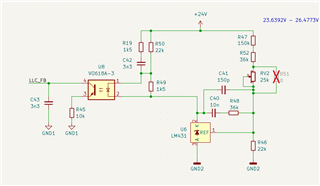
    THX for your great help, it took me some time to study but man now my initial pot seems bad.

    Anyway I did tune a bit the values of the compensation circuitry with what u have on the eval board since those are probably close enough and they study R46 R47  and if going X10 there is ok since you used about x10 in the eval board . LM431 needs like 1-uA on ref pin and with about 100uA flowing through the FB i should be fine or rather resistor tolerances will affect me more

    Also i mentioned over current protection long ago and how to add it in this circuit, i will research available options and the decide current sense method then return here.

    Shunt + INA amp or hall effect IC  what do you recommend? ( or something else ? ) ill also study this problem a bit

    NOW there is still something that i dont understand regarding the LLC IC:

    Tset pin programing , since there is a graph in the provided excel file ( TI IC page) ad it is Vfb vs Pin and it is not clear if i should aim to have it be a steep line or as shallow as i can get.

    There is also the problem* of start up from mains but that will be another thread since from what i understand the UCC256601 can start alone and then power itself and the APFC through a secondary winding. BUT I am not sure if this is the best way + under-voltage / enable thresholds  might not help me ( unless i set them low but then if there is a problem with APFC it could potencialy be harder to tell.

    PS also aligned more or less the compensation with the eval board with values i had on the pcb already

    Regards

  • Hi Dietrich,

    Also i mentioned over current protection long ago and how to add it in this circuit, i will research available options and the decide current sense method then return here.

    Shunt + INA amp or hall effect IC  what do you recommend? ( or something else ? ) ill also study this problem a bit

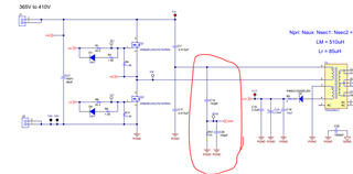
    The UCC25660x does provide over current protection by sensing the resonant tank current. You need to use RC differentiator circuit as shown in the EVM schematic. 

    Tset pin programing , since there is a graph in the provided excel file ( TI IC page) ad it is Vfb vs Pin and it is not clear if i should aim to have it be a steep line or as shallow as i can get.

    TSET resistor values mainly depends on the minimum switching frequency of operation and the OCP threshold (3.5V or 4V).

    set pin programing , since there is a graph in the provided excel file ( TI IC page) ad it is Vfb vs Pin and it is not clear if i should aim to have it be a steep line or as shallow as i can get.

    Need to make sure at max power, lower input voltage of operation, FBReplica is below the OPP threshold (4.75V). So, the slope of the curve doesnt matter as long as you follow this method

    There is also the problem* of start up from mains but that will be another thread since from what i understand the UCC256601 can start alone and then power itself and the APFC through a secondary winding. BUT I am not sure if this is the best way + under-voltage / enable thresholds  might not help me ( unless i set them low but then if there is a problem with APFC it could potencialy be harder to tell.

    .

    601 does have a HV startup so you dont need to use any auxiliary power supply. once the controller starts switching, auxiliary winding of the LLC powers up the IC. This is very efficient and low BOM type implementation.

    I am not sure what undervoltage you are talking about? Could you clarify?

    Regards

    Manikanta P

  • HI Pallantla,

    Here my architecture:

    UCC28180DR APFC  -->  UCC256601 LLC
    The LLC can start alone from the HV pin but the AFPC can t  so in order for the entire system to start it needs to have enough voltage on the UCC256601  to start i would need enough voltage on the BLK pin 357v bulk

    BLK  
    BLK Pin Stop Threshold VBLKstop 1.00 V  
    BLK Pin Start Hysteresis VBLKstarthys 0.10 V  
    BLK Pin Current Sink IBLKsink 5.00 uA  
    Desired Bulk Start Voltage VBLKStart 350 V  
    Nominal Bulk Voltage VBLK 390 V  
    Resistor Divider Power Consumption Budget PBLKsns 15 mW Enter the desired power consumption for resistor divider
    Total BLK Sense Resistor Value RBLKsns 10.14 MΩ  
    Recommended Lower BLK Sense Resistor Value RBLKlower 37.24 kΩ  
    Actual Lower BLK Sense Resistor Value RBLKlower 36 kΩ Enter the actual value of the lower BLK sense resistor used
    Recommended Upper BLK Sense Resistor Value RBLKupper 10.10 MΩ  
    Actual Upper BLK Sense Resistor Value RBLKupper 10 MΩ Enter the actual value of the upper BLK sense resistor used
    Actual Bulk Start Voltage VBLKStart 357 V  
    Actual Bulk Stop Voltage VBLKstop 279 V  
    Actual BLK divider power consumption PBLKsns 15.155 mW

    Then again there is a start sequence , i am a bit afraid not to be caught in a trying to restart loop

    This https://www.ti.com/lit/df/tidmd32/tidmd32.pdf?ts=1732469262559

    seems to also start the LLC first then the APFC so maybe i was overthinking.

    With this not much is left to ask but still a lot of work , i need to add a fan for cooling and a few leds for indicators (current on load) + layout.

    I hope i dont have other questions.

    Best regards

  • Hi Dietrich,

    Whats your output voltage and current range? and what's the application? I will let you know the startup sequence should be based on your response.

    Regards

    Manikanta P

  • Hi Pallantla,

    Output is 24V* DC  10-10.5A ( aim was 10A but i did all math with 10.5 + design margin so 10-11A in practice probably ) . It is power rail for other things but primarily for charging batteries (with a external charger ). And if one is available then for other general stuff like maybe draw a bit for a small pump ( since if i have a space power supply why not? ).

    Later when i deal with a much more powerful power source i wanted to have had some experience with this level of power and design ( since adding a custom transformer can make things way more unpredictable ) the current design is based on a commercially available transformer so that i know it should work. It usefully project that was moderately ambitious but thought me a lot ( before i get into higher voltages and currents ) and from what you probably saw from this thread there was a lot to  learn. Dealing with tons of new stuff is hard but now i think i can handle more in the future.

    As a long term goal i want to make something isolated bidirectional but that is WAY out of my leagues so for now 1 way is enough, if it works now i can make another board with a more appropriate transformer and now a good idea what i am doing on the LLC side. (there is a very strong possibility that i can make it work with just some more gain but i am still limited in current).

    PS i had a though regarding current and i will add a shunt+ INA for my monitoring purposes since i want another data set, not only my active loads.

    Anyway THX for the great help

    Best regards,

  • Hi Dietrich,

    In this case, you could use HV start of the LLC IC to charge the VCC caps of both PFC and LLC controllers. Initially PFC controller starts switching when VCC voltage reaches VCC turn on threshold voltage. Once the PFC output reaches LLC strart up threshold (
    close to 390V), LLC controller will start switching. You dont need to use any external flyback converter to power up the both the controllers. After the LLC start switching, VCC of PFC and LLC are supplied by the aux winding of the LLC. Let me know if you have further questions.

    Regards

    Manikanta P