This thread has been locked.

If you have a related question, please click the "Ask a related question" button in the top right corner. The newly created question will be automatically linked to this question.

TPS25751: TPS25751 design check for usb datalines

Part Number: TPS25751
Other Parts Discussed in Thread: BQ25792, , TS3USB221A

Tool/software:

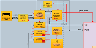
In our design we are using the TPS25751 as the PD controller and the BQ25792 as the battery charger IC. Currently, the USB data lines are connected directly to the PD controller, which then routes them through a MUX. This allows the data lines to be split, by default, to the battery charger IC and then to the microprocessor for data transfer. We are uncertain if this configuration is optimal for our design. I have added our architecture—could you please review it to confirm if this design approach is correct?
  • Hi Jefin, 

    Can you elaborate why the USB data lines need to be muxed from the USB Type-C connector to BQ25792? Is this specifically for BC1.2 support or other project requirements?

    Thanks and Regards,

    Raymond Lin

  • Hi Raymond,

    The MUX is placed after the PD (Power Delivery) controller to route the USB data lines default to the BQ25792 or to the processor. When charging, the MUX directs the data lines to the BQ25792 to support BC1.2, allowing the BQ25792 to detect the charger type and set the appropriate charging current. For data transfer, the MUX switches the data lines to the processor, enabling communication. This setup allows the USB Type-C connector to handle both charging and data functions efficiently.

  • Hi Jefin, 

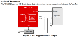
    TPS25751 has the capability to enumerate BC1.2 through its GPIO4 and GPIO5, see block diagram below for reference: 

    You do not need to connect the DP/DM lines from the USB-C connector to BC25792, instead you can route them to TPS25751 and during BC1.2 contract TPS25751 will configure BQ appropriately. 

    Thanks and Regards,

    Raymond Lin

  • .

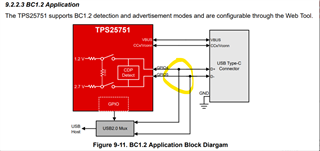
    How to connect the DP/DM lines from the USB-C connector to the processor effectively? Specifically, is placing the MUX in the highlighted position the optimal solution, or would you recommend an alternative placement or setup to ensure efficient functionality for both data transfer and charging?"

  • Hi Jefin, 

    For USB2 data, the DP/DM lines can be shorted together while connecting part of the USB2 lines (DP/DM) to GPIO4/5 of TPS25751 for BC1.2 enumeration. Upon connection, TPS25751 will enumerate BC1.2 protocol (depending on the connection made, TPS25751 will enumerate as either a BC1.2 source or sink) and configure the selected BQ accordingly to deliver/charge on the agreed charging protocol. After BC1.2 contract is made, TPS25751 does not use the DP/DM lines for anything else (unless configured for DCP schemes). 

    The USB2.0 mux shown in the block diagram is dependent on your end application, in most designs for USB2.0 the DP pins from the connector shorted together (same with DM lines) similar to how a USB-A connector only has one set of USB2 data line (VBUS, DP, DM, and GND pins). If a mux is needed to change where the DP/DM lines are connected to in the system, TS3USB221A is an example of a USB2 mux: https://www.ti.com/product/TS3USB221A 

    Otherwise if there is only one USB endpoint in your system, the DP/DM lines can be routed directly from the connector to the MCU.

    Thanks and Regards,

    Raymond Lin