This thread has been locked.

If you have a related question, please click the "Ask a related question" button in the top right corner. The newly created question will be automatically linked to this question.

BQ25756: Battery back-feed to input when reverse mode is disabled

Part Number: BQ25756

Tool/software:

Good Morning,

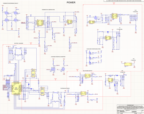
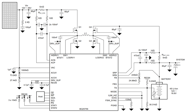
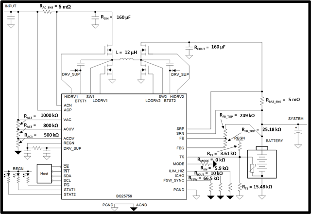
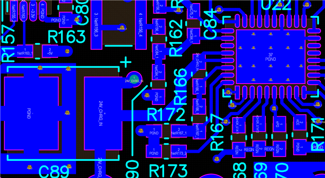
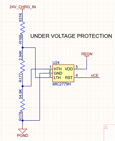
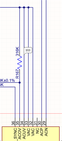
I have 75 CCAs with the BQ25756 handling battery charge (preferably stand-alone when the processors are off). In approximately 50% of the CCAs, I have run into an issue where the battery appears to be boosted and back powering the input supply when the input supply is disconnected. Referencing the sample circuit on page 71 of the datasheet, I am seeing the following results on the CCAs that are acting unusual (the other 50% are behaving exactly as would be expected and the problem is not intermittent):

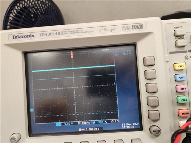
  1. Battery Voltage = 22.2V
  2. VIN = 23.5V
  3. Q4 Drain = 22.2V
  4. Q4 Source = 21.5V
  5. Q1 Drain = 23.5V
  6. Q1 and Q4 have a PWM with a low duty cycle present
  7. REGN = 5V
  8. STAT1 = 0V
  9. STAT2 = 5V

The following register results are on the I2C when the problem is occurring and the processors are communicating

  1. Reg 17 = 0xC9
  2. Reg 19 = 0x20
  3. Reg 21 = 0x2B
  4. Reg 22 = 0x80
  5. Reg 23 = 0x00

I can get the back-feeding to stop by performing any of the following:

  1. Disconnect the Battery
  2. Increase/Decrease the thermistor temperature outside of threshold
  3. Set Reg 17 to 0xC8
  4. Add a large load to the input source

When I do any of the above 4 actions, the BQ25756 stops charging and powers off (REGN = 0V). I originally believed that the device was entering reverse mode; however, after observing the REGN at 5V and the registers reading Full Charge Mode (CC) while REV_EN =0, I stopped believing this to be true. I am concerned because 50% of our lot appears to be performing as expected while 50% seems to be failing in the same manner. If a copy of the schematic for the use case or pictures of the signals will be of any assistance, please let me know and I will provide them. Any assistance with this problem would be greatly appreciated.

  • Hello Eric,

    Thanks for being patient with this. I'll get back to you on this thread question tomorrow.

    Best Regards,
    Ethan Galloway

  • Hello Eric,

    Thanks for the detailed testing results. This is a strange behavior to have.

    I see the charger is VAC_DPM. VAC_DPM probably keeps the voltage source on VAC from completely depleting.

    I've got a few questions to help us debug this:

    • Can you send me the schematic?
    • When you set Reg 17 to 0x18 to stop charging, what voltage do you see on VAC at that point?
    • Is there any potential source of voltage that could feed into VAC? For example, does VAC have a large set of capacitors on it?

    Best Regards,
    Ethan Galloway

  • Ethan,

    I will attach a screenshot of the schematic. If it is better, I can also attach the .schdoc if you request that. When Reg 17 is set to 0xC8, The voltage on VAC drops to ~0V within a few msec. There is 220uF input filter capacitance on the VAC line as you can see on the schematic. The Input VAC is being fed by an inductive wireless charger. 

    Thank you,

    Eric

  • Some new info as well. We have discovered that this problem only appears to happen when our battery is between ~20.5V and ~23.24V

  • Hello Eric,

    I've got another testing idea. Maybe voltage is leaking through your FETs?

    Can you measure the resistance from BAT to VAC on a failing unit?

    With only VBAT plugged in, what's the voltage on VAC with a failing unit with Reg 17 = 0xC8?

    Also, I'm looking at your schematic and I see REGN connects to DRV_SUP through a 10Ω resistor. We normally recommend connecting REGN to DRV_SUP directly if the internal gate drive is being used. If you short R71, does anything change for a failing unit?

    Best Regards,
    Ethan Galloway

  • Ethan,

    The FETs are being turned on by HIDRV and LODRV. There is a very low duty cycle PWM on those. Resistance from VAC to BAT is 32MOhm when off and variable when on. VAC voltage when only VBAT is connected and Reg 17 = 0xC8 is 6mV. We used the below examples for the REGN to DRV_SUP (from the calculator and design documents provided by TI). No changes when R71 is shorted. Below is an explanation of the problem we are seeing if it helps. We are seeing this problem on all CCAs now, it was only apparent during a certain voltage level of the battery and each has a slightly different window based on tolerances of R166. 

    Problem Statement

    The wireless power receiver LEDs will stay lit when the receiver is not aligned with the power transmitter, or the power transmitter is turned off.  The receiver LEDs must then be powered from the battery reducing the SOC and is visible to the customer.

    Diagnosis

    Registers were evaluated in the BQ25756 charger ASIC and MOSFET measurements were taken.  It was confirmed that the charger MOSFETs were being switched when in this condition even though there wasn’t a power source driving the charger. 

    When in the fault condition, register 0x21 (Charger Status 1) has bit 5 set which is input voltage regulation status.  Two conditions can cause this bit to be set VAC_DPM or VSYS_REV.

    VSYS_REV occurs when the converter operates in ‘reverse’ mode which bucks/boosts from the battery to the output.  It was confirmed in register 0x19 that EN_REV (Bit 0) was set to 0 and a read of the register confirmed it was 0, meaning this ‘reverse’ mode is disabled.

    VAC_DPM (Input voltage dynamic power management) causes the charger to reduce input current to reduce sag in the input voltage.  The control input for this regulation is the ACUV (input voltage undervoltage pin), which is dual-purpose providing the input for both DPM and Undervoltage detection.

    It was found that if the DPM state was entered, the charger would reduce input current down to 0 amps in order to regulate the input voltage to the DPM setpoint.  That would normally be OK, however, when a buck regulator is operating, it effectively acts as a boost regulator to the source (boosting looking into the source, bucking looking into the output).  The system reaches equilibrium where the charger has reduced input current to 0 while the parasitic input boost keeps the ACUV pin above the ACUV threshold.  The regulator keeps running in this condition which provides power to the wireless power receiver.

    The undervoltage threshold calculates to 21.43V nominally, under which the regulator shuts off as expected.  The DPM threshold calculates to 23.57V nominally, which causes input current regulation at or below this point.  If the input voltage regulation is operating and power is removed, the switching provides enough boost to the input to keep it above the 21.43V undervoltage threshold.  There is no way to disable the DPM functionality with software.  It can only be disabled by tying the ACUV pin to the input voltage (VAC), which also disables the onboard AC

    One big clue in my opinion is that the circuit only enters this state when VBAT is between ~21.5V and ~23.5V. When outside of that range, I cannot get the CCA to enter the failure state. Below are seen during the failed state

    Q19 pin 8

    Q19 pin 2

    Q19 pin 4

    Q19 pin 5

    Q20 pin 4

    Q20 pin 2 is low

  • Hello Eric,

    Thanks for the very detailed analysis. I will look into this and get back to you later this week. Thanks for being patient with this.

    I've got a question in the mean time. Have you tried an ABA swap? In other words, if you take an IC out of a bad board and put the IC into a good board, does the good board still work? And if you take an IC out of a good board and put it into a bad board, does the bad board still fail?

    Best Regards,
    Ethan Galloway

  • Ethan,

    We were about to try an ABA swap when we discovered that all the CCAs actually enter the failed state, just at slightly different battery voltage windows and we also discovered that the "bad" CCAs were working properly during the majority of the battery SOC stages, We determined that the "window of failure" changes based on actual resistance of R166. Even with a 1% tolerance, that means the  resistance can change up to 3.16K and that changes the SOC level that enables DPM mode on the circuit. So after that explanation, the short answer is we determined that it would not be prudent to time constraints and effort to perform an ABA swap. Due to time constraints for product shipment, we have implemented a software change that monitors REG 19 bit 5 and if the processor detects a 1 for 3 seconds, it will set REG 17 to 0XC8 then back to 0xC9 which solves the issue for 95% of our use case and we implemented another software "patch" that turns off the VAC Supply circuit prior to the processor power down that solves our issue for another 3% of our use case scenarios. We still have a 2% chance that the system will enter this state and will be disabled after 24 hours with the timer. We are implementing a circuit change to bypass the ACUV and DPM function by placing our own Input source monitoring and controlling the charge enable line to fix this due to time constraints and customer needs; however, I am still very interested in a TI solution to this problem for future use of this component. We won't likely use this component again unless there is a TI solution. Thank you for continuing to work with us toward finding a solution.

  • Hello Eric,

    Thanks for the update and thanks for working through this. I've never seen anything like this before and I've been unable to replicate your results in the lab.

    By the way, I've been looking through your schematic again and I can't find the capacitor for the VAC pins. We normally recommend installing a 1uF on the VAC pin to filter out noise and stabilize power for the chip. Is this capacitor in the circuit? If this capacitor is not installed, does installing the capacitor fix the behavior?

    I also recommend installing an RC filter in parallel with the ICHG resistor when this resistor is greater than 5kOhm. However, this RC filter shouldn't effect the input voltage divider.

    Best Regards,
    Ethan Galloway

  • Ethan,

    I decided not to add the 1uF bypass cap because I figured we should be pretty safe since as you can see below, the 100uF tantalum input filter cap is within 300 mil of the VAC pins. With that being said, I will add the 1uF bypass cap and update this post appropriately. I suspect it won't change much as it will mainly filter out high frequency noise. The inductive wireless charger we are using does have ~400uF output filter capacitance but it is separated by approximately 2 feet of 12AWG wire. Do you think this capacitance could be holding up the VAC line just long enough to cause this state? If that is the case, why would it only be when the battery is at a specific SOC window? Is there a way to permanently disable DPM mode? If we could disable this mode permanently, it would solve our issue and we do not need DPM mode as our input source is well regulated.

    Thank you,

    Eric

  • Installing the 1uF between Pin 33 and PGND had NO impact on the symptoms.

  • Hello Eric,

    Thanks for the tip about the 400µF capacitor. I've added a large capacitor on the input of my setup and I've managed to replicate your results in the lab. I'm still investigating this.

    I think removing or reducing those 400µF capacitors will remove the boost-back behavior.

    Do you think this capacitance could be holding up the VAC line just long enough to cause this state?

    Yes, I think this is the culprit at the moment.

    Is there a way to permanently disable DPM mode?

    There's no way to disable the DPM mode.

    If that is the case, why would it only be when the battery is at a specific SOC window?

    I'm looking into this.

    Best Regards,
    Ethan Galloway

  • Hello Eric,

    I've found a few more conditions that will stop this behavior:

    • A diode between the distant capacitance and the charger's VAC capacitance will stop this problem.
    • Setting EN_IAC_LOAD=1 will also stop this condition. This may be less practical for your system though.

    Best Regards,
    Ethan Galloway

  • Ethan,

    We have already addressed the idea of a low-loss (0.4V Vf) schottky in line with the VAC input positive. We are concerned about the power consumption and heat that will be generated by the diode. Please see below for our current solution:


    In addition to this, we will tie ACUV to VAC and change the value of R167 as follows:

    This should bypass DPM mode and still allow us to monitor for under-voltage by triggering nCE in an under-voltage condition. If you have any other potential solutions that will work when power is not applied to the interacting processor and not produce as much power loss or heat, I would love to hear them. Otherwise, I will consider this closed and move forward with our current application.

  • Hello Eric,

    Thanks for letting me know about this. I'm going to mark this thread as closed for now.

    I have no further suggestions at the moment, but I am still looking into this in lab. I will let you know if I find anything else that may help your system.

    Best Regards,
    Ethan Galloway