Tool/software:
Hi there,
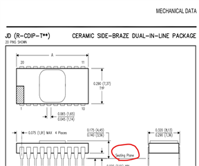
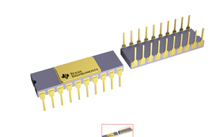
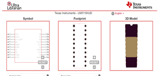
I am looking for thermal pad/via information for LM5116-HT.
I cannot find useful information in the datasheet about that topic.
I am designing a PCB which will work in high ambient temperature conditions (150ºC-175ºC), so the design needs to be as accurate as possible to minimize risks. There are some questions about that topic:
How many vias is desireable to put? what is the size of the thermal pad where thermal vias will be located? How many space is necessary between them?
AGND and PGND should be connected by a NET TIE? If yes, where is a good location (low impedance location) to put it?
Thank you in advance.
Best regards.


