This thread has been locked.

If you have a related question, please click the "Ask a related question" button in the top right corner. The newly created question will be automatically linked to this question.

TPS61289: TPS61289 design review

Part Number: TPS61289
Other Parts Discussed in Thread: INA219, TPS25947

Tool/software:

Hi team,

So after the GREAT support i got here https://e2e.ti.com/support/power-management-group/power-management/f/power-management-forum/1423648/tps631000-searching-for-a-bidirectional-dcdc-smps/5458962?tisearch=e2e-sitesearch&keymatch=TPS61289#5458962 

I have returned with a more or less finished schematic to check if all is ok.
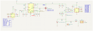
so F1 is rated for 3A hold current and my desired continuous current is 2A (3A maybe later if all is ok and the IC is not to hot)

Both the SMPS control pins are toggled by a MCU, it also reads the INA219 and controls the DAC . There is a opto coupler that acts as an emergency disable for the SMPS in case it is ON for some reason when i cell in inserted in reverse ( it should not be but it is a safety mechanism) . There is enough series resistance to not overdrive the MCU pin of the opto is active.

D6 is probably redundant since the opto coupler can handle 6V in reverse voltage.

Addresses are set on a higher LVL schematic ( there a multiple blocks like this on the 24V bus, there is also a INA219 on the 24V bus that will sum up net current going in and out of the board and some bus protection like a fuse.

Vref is 1V6 in schematic but we can adjust it, i am heavily considering going with 1V8 since it is a way more common voltage value.

From what i understand in the datasheet with Vhigh stuck at 15-25V and Vlow in the 2.5-4.5V range my switching frequency will stay constant at 250kHz. all inductor math was done with this value only.

1 Output and input capacitance are from EVAL board val;ue scaled  for my current , there is no calculator or datasheet formulae, EVAL is at 10A and i need 2A so i more or less did a  /5 on the capacitance.

There seems to be enough free space and i could add  a few more footprints and decide to populate or not..... ( this in on Vlow )

2 On Vhigh ill do the same and in a way all blocks share capacitance so i am not sure, considering adding some big caps between adjutant blocks. What do you think ?

3 R20 Current limiting resistor , 20k is for full 20A , form datasheet.  Regarding the formula i am not sure what you mean by Valley current.

Using provided formulae from TI in boost mode we have:

Inductor_dc_current_max[A]

5.56

Inductor_peak_current_max[A] 1.63

and in Buck mode :

Inductor_dc_current_max[A] 0.67
Inductor_peak_current_max[A] 8.10

Those are the largest value given the worst possible conditions for buck and boost mode.

and if i apply the inductor saturation current formula we get  9.6A , the inductor can handle that + safety margin larger the inductor tolerance.

What current do i use for the current limiting resistance for both buck and boost mode ? For buck it is the peak* so i assume 8.1A, and for boost what is this valley current ? Is it peak + DC ?

Or should i go with 10A just to be safe and see what value i get from there? -R20=40k in this case

NOTE the (k) in the formula makes it VERY confusing since initially i though Rlim is in kohm and ended up with 40Mohm and that was very unrealistic, after i tried for 20A i figured it out

4 D1 is mostly for debug + place to put measurement test points

5 Any obvious mistakes on the schematic ? Or is there any things that i could do better and cough  your attention?

6 For preventing damage when a cell is placed in reverse do you have any small size solutions better then the fuse?

  • Hi Dietrich,

    Thank you for reaching out again.

    For your questions:

    1. the battery side's capacitor influences the current ripple; the value is to guarantee most of the ripple current is absorbed by ceramic capacitors and the current senses only the DC value. It looks ok.

    2. For the VHIGH side, the capacitor is to guarantee the voltage stable, and you could choose the capacitor with 1% voltage ripple.(by calculating the charging/discharging current)

    3. For the current limit, the value is ok with 40k value, which set the limit to be 10A.

    For boost mode the limit is valley.

    For buck mode the limit is peak.

    the inductor's peak-to-peak current can be estimated as 1A.

    As a result, the device will actually limit the DC current of 10.5A at boost mode and DC current of 9.5A at buck mode.

    The demanded DC current is about 2A, which is just the battery current.

    So, the current limit can further be decreased to 6A.

    4. it is ok.

    5. the FB voltage is set to be 0.7V may be wrong

    As I said before, the FB voltage decides the comp pin current direction.

    When it is below 1V, the comp will source current.

    For your case, the output is connected to a DAC and it could be hardly sink current (please check this), and the comp cannot be stable.

    It is recommended to set the FB higher than 1V(in all VHIGH range), to make comp pin sink current to meet the DAC port.

    Also to ensure the DAC output current is higher than COMP pin sink capability 20uA(maybe more to leave more margin).

    6. TI has some devices for prevent battery reverse and over current.

    7. I have some questions about the design.

    Are D6 and U1 designed to prevent battery reverse?

    What does the Vref 1V6,1V8 referring to? I didn't see anything like that.

    Please change the R22 to 0ohm first to ensure a quick driving waveform, as well as decrease the switching loss.

    Also, the powering sequence is important. Vhigh and Vlow voltage are recommend presenting before EN going high.

    Then DAC output stepwise from 0V to a typical value.

    Please tell me if you have more questions.

    Best Regards,

    Fergus

  • Hi,

    THX again for your great support, here are my answers:

    1&2  yea that is the same as a formal SMPS

    3 6A gives 66k and 7A gives 57k so i made R12  56k just to be sure that is like 7A and a bit extra

    4 great

    5 i followed the datasheet and what we talked last time....

    regarding the DAC it has a buffered output ( +-10mA continuous if i understand well this https://www.ti.com/lit/ds/symlink/dac121c085.pdf?ts=1731524078838&ref_url=https%253A%252F%252Fwww.google.com%252F )

    Please also check , if you think there is a problem then it is just a resistor  value that i need to change so that is fast&easy

    6 I saw there are some Efuses that can do some stuff but i had a hard time filtering something that is a 1 IC solution and also potentially hand solder able ( non BGA ) , maybe in the load switch category there is something....

    ( will check TI portfolio tomorrow) I am also very open to recommendations

    7 it is a safety disable for the SMPS just in case the SW does not stop the SMPS the opto will

    the DAC is a DAC121C085CIMM/NOPB (long name/code that is why i hid it LOL i was now like why did i hide on TI forum the use of a TI part from TI ), and the 1v6 and 1v8 would be the voltages used for powering the reference of the dac

    1v6 is double 0.8V and that is some value i got from the datasheet for COMP pin when idle ( R17 was also sized to 30k so that i could bet +-20uA between the DAC and COMP pin ) but based on point 5 i am not sure anymore..

    R22 is now 0 ( i want to have some control and a easy probe point, else i would be tempted to use via in pad.... )

    regarding the start sequence that good to know since that can be baked into the SW i have a 10k pull down on the enable to make sure i start off regardless

  • Hi Dietrich,

    Thanks for the information.

    For the DAC and comp connection, it seems ok when the DAC is capable of sinking such current.

    And the FB resistor does not need to change.

    the comp voltage directly controls the inductor current, as a result, 1.6V means the max controlled current 20A.

    1.6V will be already enough current for your application.

    I'm not familiar with the e-fuse, either. 

    You can reach out to our FAE or submit another E2E if needed.

    Best Regards,

    Fergus

  • Hi Fergus,

    THX for your help.

    I did some research on eFuses and here is what i came up with:

    https://www.ti.com/product/TPS2521?dcmp=dsproject&hqs=#order-quality
    TPS25947 
    https://www.ti.com/product/TPS2521

    It is only for the cell so i think it is good enough but i am still seeking another opinion,

    What do u think?

    Besides this i am done with schematic and now only doing layout and very excited to test this board.

    Best regards,

  • Hi Dietrich,

    Both look ok and fit for your application.

    Either is ok and I do not have any more suggestions.

    Looking forward to see your board and test result.

    Best Regards,

    Fergus