This thread has been locked.

If you have a related question, please click the "Ask a related question" button in the top right corner. The newly created question will be automatically linked to this question.

TPS2640: TPS2640, LM76005 and LMR51430 PCB Placement and Layout Design validation

Part Number: TPS2640
Other Parts Discussed in Thread: LMR51430, LM76005,

Tool/software:

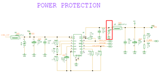
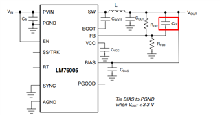
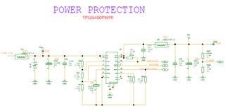
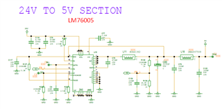
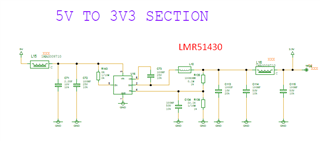
We are designing a custom PCB with 24 V input. we used TPS26400PWPR for power supply protection. LM76005 is used to convert 24 V to 5 V and LMR51430 is used to convert 5 V to 3.3 V. (https://e2e.ti.com/support/power-management-group/power-management/f/power-management-forum/1429731/tps2640-design-validation-for-power-section)

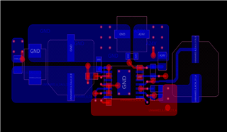
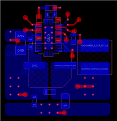
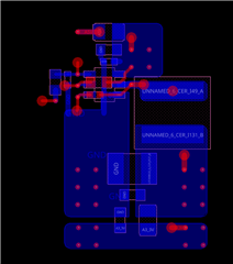
Below are the screenshots of the circuit (schematic and PCB). Please validate the PCB Component placement, layout design and suggest if any modification is required.

The Power requirement for each rail is as follows:

24V rail: 1A max

5V rail: 3.5A

3.3V: 2A


Thanks.

  • Hello Akash,

    Consider adding a Schottky diode at output for negative voltage ringing for TPS2640 as suggested previously.

    OUT pin can violate negative voltage abs max. 

    Layout is fine.

    Thanks

    Amrit 

  • Hi Akash,

    For the LM76005,

    1. Add another 4.7uF capacitor to the input VIN rail
    2. What is the purpose of C136?
    3. Consider adding a layout placement for a feed-forward capacitor between VOUT and VFB
    4. What is the inductor value of L11? I suggest following the datasheet of using a 6.8uH inductor for this application
    5. Depending on the expected load step transient behavior, reducing output capacitance to increase the loop bandwidth is an option. See attached quickstart calculator. 
    6. Layout looks good.

    LM76005-Q1 quickstart tool - rev A_Akash.xlsm

    Ben

  • Hi Amrit and Ben,

    Thanks for your valuable suggestions.

    For TPS2640: I have added the Diode (D25, P/N- SK36BHE3-LTP). Below is the schematic for your reference.

    For the LM76005:

    1. As suggested, we will add another 4.7uF capacitor in parallel to C116.

    2. C136, 0.1uF Cap in Feed back path is for good dynamic reference. Is it fine?

    3. For feed-forward capacitor (CFF) between VOUT and VFB, can I add 47pF capacitor as suggested in application circuit in datasheet?

    4.  The L11 as per webench simulation for 24VIN-5VOUT, 3.5A is 5.6uH (Below image). So, We have connected a 5.6uH, 10A inductor (SRP6060FA-5R6M) in this design. Should I need to change it to 6.8uH?

    5. Regarding load step transient behavior, the output capacitor values are taken from the webench simulation results. Shall I need to reduce it to 125uF as suggested in quickstart calculator?


    Also, Waiting for TI response for LMR51430.

    Thanks.

  • Hi Aakash,

    2. C136, 0.1uF Cap in Feed back path is for good dynamic reference. Is it fine?

    From a frequency point of view, adding C136 will add a pole at a higher frequency which will lead to lower gain of the loop. From a transient point of view, the loop response will be a lot slower. I suggest adding C136 to the layout as a DNP (do not populate) so the board has the option to add the capacitor if needed.

    3. For feed-forward capacitor (CFF) between VOUT and VFB, can I add 47pF capacitor as suggested in application circuit in datasheet?

    Excellent

    4.  The L11 as per webench simulation for 24VIN-5VOUT, 3.5A is 5.6uH (Below image). So, We have connected a 5.6uH, 10A inductor (SRP6060FA-5R6M) in this design. Should I need to change it to 6.8uH?

    Yes, I would follow the datasheet recommendations.

    5. Regarding load step transient behavior, the output capacitor values are taken from the webench simulation results. Shall I need to reduce it to 125uF as suggested in quickstart calculator?

    Yes, only if the inductor value is at 6.8uH. A larger inductor value will have a smaller inductor current ripple so the design can tolerate a lower output capacitance. Just add a few more layout landings so the output capacitance can be increased if needed during evaluation.

    Ben

  • Hi Aakash,

    For the LM76005 device, are there any other questions or updates? If not, please close the thread by clicking on "resolved". Thanks,

    Ben

  • Hi Ben and Amrit,

    Thanks for your valuable suggestions for TPS2640 and LM76005. Those two sections are clear and I will try to share the updated schematics and layout.

    I am just waiting for feedback on LMR51430. If there is anything to be modified for this section please let me know.

    Thanks.

  • Hi Aakash, 

    Thanks for the update.

    Ben

  • Hi Aakash,

    Are there any updates?

    Ben

  • Hi Ben and Amrit,

    Thanks for your valuable suggestions for TPS2640 and LM76005. Those two sections are clear and we have updated in the Schematic & PCB.

    I was just waiting for feedback on LMR51430. But, I didn;t get any feedback for this. I have followed the datasheet design guidelines for the same.

    Thanks.