This thread has been locked.

If you have a related question, please click the "Ask a related question" button in the top right corner. The newly created question will be automatically linked to this question.

LM3485 EMI Issue

Other Parts Discussed in Thread: LM3485

Hello All,

I am FAE of TaeHo Kim in TI Central regional  KOREA.

My customer is Hansol tecnics which is developing the SMPS for LED TV.

The end user is Samsung VD in Korea.

They have got an EMI issue.

I send PCB pattern and LM3485 circuit.

Could you review the attached file?

If you find out some EMI problems from pattern or circuitm, reply to me by e-mail please.

Specification

  Input DC voltage: 12.8V

 Output SPEC: 5.3V/3.5A

Thank you.

buck_ic_pattren and circuit.xlsx
  • Hi

    'Radiation' point of view, the loop area in which a discontinuous current flows should be minimized.

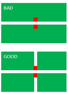
    Right now, input capacitors are a little bit away from high side switch and freewheeling diode.  This can be improved by placing a SMD ceramic capacitor (2.2uF or 3.3uF, check temperature) very close to the source connection of MDD3752 and the anode connection of MBRF10U.

    'Conduction' point of view, please see below about input capacitor connections.

     Hope it helps.

    Regards,

    Eric

  • 6683.buck_ic_pattren and circuit.xlsx


    Dear Eric,

    Thank you for your answer.

    My customer ask to add something. 

    For the customer want to solve the EMI problem, they added  one bead-core on MBRF10U45 Cathode.

    So the EMI is reduced, but they worry about another issue.

    The MDD3752 drain voltage  has got a spike negative voltage.

    So is it O.K? is it create another problem?

    Could you review the attached file please?

    Thank you for your attention.

    Best regards.

  • Hi

    Absolute maximum rating of ISENS is -1V to 36V. I see about -9V spike at falling edge. LM3485 might be abled to be survived during prototype evaluation , but it will bring a reliability issue eventually. .   

    Current limit comparator has approximately 100ns blanking time. VDS should reach its target volage within the blanking time when VDS sensing being used.

    Use INTERNAL FORUM.

    Regards,

    Eric

  • Tae Ho,

    I don't recommend placing the bead there. The negative spike is too large and can cause improper operation or damage.

    I  recommend adding ceramic input cap connected close between the PFET source and diode ground. Adding more ceramic cap here helps a lot. Multiple values of cap will be more effective than a single cap.

    Second, you can slow down the switch rise time with a small resistor in series with the PFET gate, 3-10 ohms should help a lot.

    If necessary, a bead can be added on the input, between the electrolytics and ceramic caps, creating a pi filter which reduces emissions significantly.

    Regards,

    Allan

  • Dear Allan,

    Could i ask a negative spike?

    Based on our customer circuit, If we got the negative spike, which part is it damaged ?

    If the negative voltage is occured from bead core, which part is it resonant with bead core?

    If some parts(inductance(?) and capacitor(?)) have been resonant with bead core, could we reduce to adjust the part value the EMI?


    Thank you.

    Best Regards.

  • Hi

    LM3485's VDS sensing requires ISENSE pin of the IC is tied to drain connection of high side PMOS switch which is switching node. Any negative voltage ringing at the switching node affects the ISENSE pin.

    At the rising edge of the switching node voltage, CD of freewheeling diode and parasitic inductance in the 'discontinuous current conduction loop' which connecting positive side of input capacitor, high side switch, freewheeling diode and negative side of the input capacitor are the major contributors of resonance.  

    At the falling edge of the switching node voltage, COSS of the high side switch and the parasitic inductance in the same 'discontinuous current conduction loop' are the major contributors of resonance.

    Regards,

    Eric 


  • Regarding the negative voltage, it is not due to resonance. When the high side switch turns off, the inductor current forces the low side diode on. This is an instantaneous change in current in the bead. Any fast change in current through an inductor causes a fast voltage change (v=L(dI/dt)).

    If you prefer to not slow down the FET with a gate resistor, the next best solution may be to add a snubber. This has a similar effect to the bead. Refer to the link below:

    http://www.national.com/en/power/snubber_circuit_design.html

    Regards,

    Allan

  • Dear Allan,

    Thank you for your answer.

    I read the your recommanded RC snubber web site.

    I am not sure about some letter such as 'Cs' and 'Cext'.

    What is Cs and Cext mean in the fonula?

    I think the Cs is a parasitic capacitor, isn't it?

    I think the Cext is a output capacitor, isn't it?

    So could you make sure these factor?


    Thank you very much.

    Best Regards.


  • Cs is the parasitic capacitance at the SW node.

    Cext is not the output capacitor. It is the value of capacitance used across the SW node to determine the required damping cap value. This procedure is described in step 1, Cext value is adjusted to cause the ringing frequency to reduce in half.

    Cs=1/3 * Cext

    Follow the example, it should be clear.

    Regards,

    Allan

  • Dear Allan,

    When I followed the example, I can't understand Why the Cext value is 330pF.

    Which fomula is the Cext value come from?

    It is not mention that.

    So could you send the fomula?

    Thank You.

    Best Regards

  • Cext means C external. You find this value by trial and error, placing in from the switch node to ground. This is the value of capacitor that causes the ring frequency to be one half of the original ring frequency.