Tool/software:
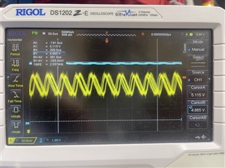
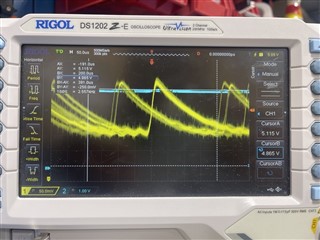
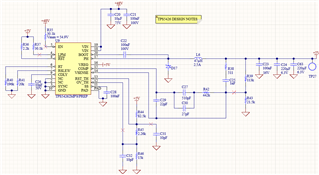
We recently found a failure mode in our design using the TPS54262. On some boards, they fail to regulate properly on startup. The signal bounces between VReg_UV and VREG_OV, making me think it is in Hysteretic mode for some reason and can't get out. Upon further inspection, there are some that startup and regulate fine at no load but then get a fairly large sawtooth (500mV p-p) at different current draws (10mA - 500mA typical). As you increase current, you can see the sawtooth signal increase and then decrease. There isn't much for a load on startup, the output runs to a 3.3V LDO that only powers a uC and a 5V switch with all ports off.
Some design parameters:
- Vin, min = 40V
- Vin, typ = 48V
- Vin, max = 55V
- Vreg = 5V +/- 1%
- Iload, max = 2A
- ∆VIN 1% of Vin
- Vreg_RST = 92% of Vreg
- Vreg_OV = 106% of Vreg
- Vreg_UV = 95% of Vreg
- ∆VReg = 5% of Vreg
- PORdly = 10ms
- Fsw = 500KHz
Some design parameters:
- Vin, min = 40V
- Vin, typ = 48V
- Vin, max = 55V
- Vreg = 5V +/- 1%
- Iload, max = 2A
- ∆VIN 1% of Vin
- Vreg_RST = 92% of Vreg
- Vreg_OV = 106% of Vreg
- Vreg_UV = 95% of Vreg
- ∆VReg = 5% of Vreg
- PORdly = 10ms
- Fsw = 500KHz
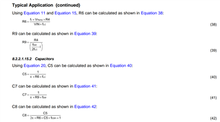
- L = 47uH
- Cout = 100nF//220uF//220uF all ceramic
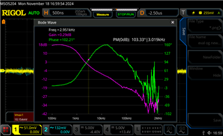
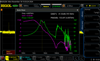
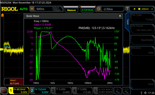
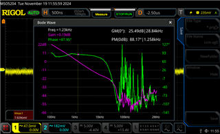
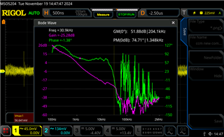
- Fz1 = 670.5Hz
- FLC = 1,106.7Hz
- Fz2 = 1,402Hz
- FESR = 244,347Hz - best guess
- Fp1 = 1,7037.8Hz
- Fp2 = 311,458Hz
We tried a slew of things on a "bad" board including (but not limited to:
- Increase soft start (no change)
We tried a slew of things on a "bad" board including (but not limited to:
- Increase soft start (no change)
- Slowly ramp voltage - works fine up to 30V, then has startup issues after that
- Various configurations of output caps - different kinds of caps, different values down to ~47uF (maybe slight improvement on sawtooth)
- Reflow all components 2x's (no change)
- Verify all component values
- Changing resistor values/caps for RST_TH and OV_TH (this drove the most change)
In the end reducing threshold resistors (R1, R2, and R3) by a factor of 5 solved all issues. R1, R2, and R3 originally added up to 100k but now are at 20k. The datasheet has two different statements on this - one says they should add up to less than 200k and another says they should add up to 100k. The theory here was there was noise on the threshold values and increasing the current increased our noise threshold (just a guess).
In the end reducing threshold resistors (R1, R2, and R3) by a factor of 5 solved all issues. R1, R2, and R3 originally added up to 100k but now are at 20k. The datasheet has two different statements on this - one says they should add up to less than 200k and another says they should add up to 100k. The theory here was there was noise on the threshold values and increasing the current increased our noise threshold (just a guess).
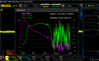
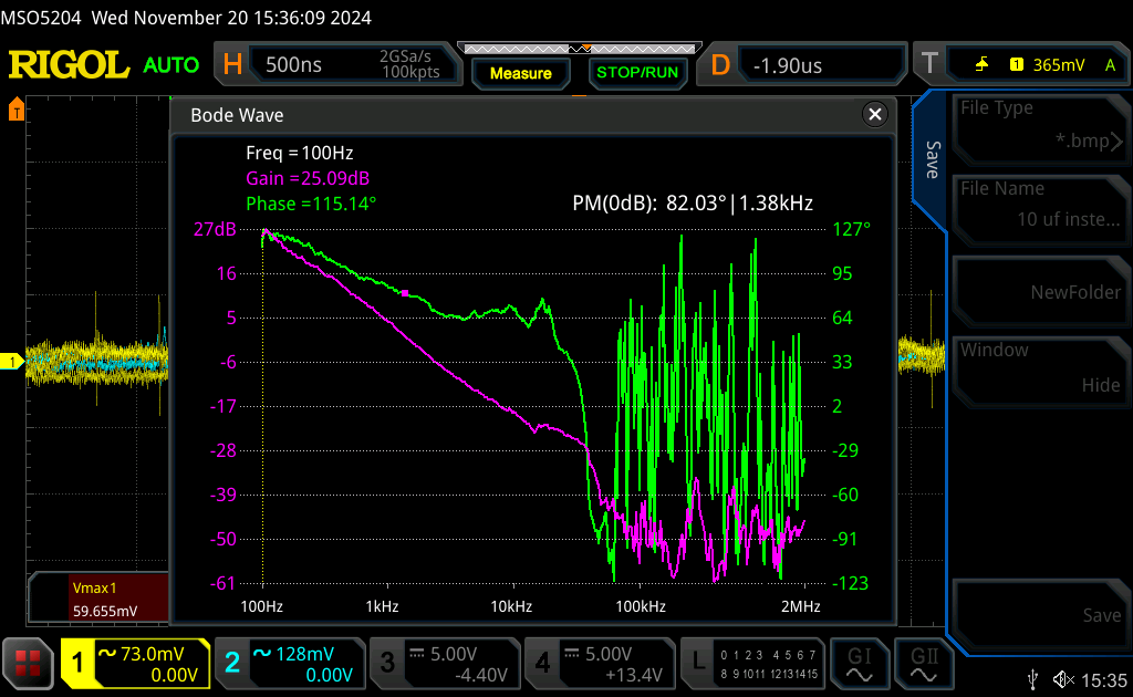
My questions are (1) is there any reason we shouldn't run with the R1, R2 and R3 at lower values? and (2) We haven't touched the compensation circuit yet and it looks like there might be room for improvement here to some degree. Looking at it on paper we aren't exactly where we should be. My fear is by changing the threshold resistors, we are somehow compensating for another issue. I'm new to these compensator circuits - I have a hard time judging if we need to get some equipment to measure this in-circuit and adjust or if the calculations are close enough and it should be good. (3) Any other thoughts to why we are seeing these issues?
Thank you for your help.
Thank you for your help.