This thread has been locked.

If you have a related question, please click the "Ask a related question" button in the top right corner. The newly created question will be automatically linked to this question.

UCC27712: Turn off time

Part Number: UCC27712

Tool/software:

Hi,

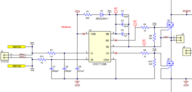
I am trying to implement a circuit using the UCC27712 based off of the PMP23338B reference design.

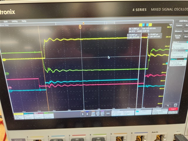
In the attached scope shot 

Yellow -- HO referenced to HS (ignore voltage scale)

green -- LO

Blue -- HI

Red -- LI

It appears that the delay to the rise time of the output signals matches the data sheet (100ns). However, the fall time is 1.6usec when it should be 100ns?

In light of this, I need to go back and look at the timing on the PMP23338B reference design when I have time. We implemented the design and noticed a lot of switching noise that needed more investigation.(off topic).

Regards,

John

  • Hey John,

    Thank you for reaching out with your questions regarding the UCC27712.

    Looking over your schematic, I do have a few questions and comments.

    1. What FETs are you using?

    2. The HB-HS capacitance is well beyond what we typically expect, this should be sized based on the FET, duty cycle, and desired ripple. These should be X7R ceramic capacitors. Please reference this Application Note:

    - Bootstrap Circuitry Selection for Half-Bridge Configurations

    3. The VDD capacitance is far too small for providing local energy sourcing and transient response. It is advised to have a VDD capacitor that is 10x that of the HB-HS bootstrap capacitor, as well as a small 100nF bypass capacitor on VDD. These should be placed as close to VDD as possible with the 100nF being the closer of the two. They should be X7R ceramic capacitors as well.

    4. The RC filters on the inputs should be maximum of 100 Ohms and 100pF.

    5. You mentioned that you are measuring HO-HS, which is good, but you are getting a mV scale. What differential probe are you using? Also, all measurements should be taken at the pins of the gate driver.

    Let me know if there are questions.

    Thank you,

    William Moore

  • Hi William,

    Thank you for the reply.

    1. The FET is an Infineon IPT60R022S7XTMA1.

    2,3,4

    The component values in the schematic were taken directly from the TI reference design PMP23338B. These values may be ok for 50-60 hz but not for 20khz. I will go back and review and update these values

    5. It is a Tektronics P5200, the true scale is 5v/div.

    I will reply again when I'm back in the office Monday and can make the updates.

    Thanks again,

    John

  • Hey John,

    Yes with the reference design switching at 50-60Hz and your system requiring 20kHz. That changes the design requirements. Please follow the guidelines from the application note for the bootstrap design and let me know if you have any questions.

    Thank you,

    William Moore

  • Hey John,

    Were you able to resolve this? Are there any further questions at this time?

    Thank you,

    William Moore

  • Hi William,

    Yes thank  you. Your suggestion cleaned up the timing issue.

    I delayed responding because I am still having some issues with ringing. If no voltage is applied on HVBUS, there is no ringing. Voltage applied (12v), it rings even though the current is very low (10ma through resistor). Updating the boot capacitor and resistor helped but there may be some issues in the layout.

    As a note, this is an H-bridge circuit. The schematic above is mirrored with the appropriate changes to the drive signals to create the opposite drive.

    My next steps involve cleaning up layout:

    • break out the high current path through the MOSFETs to have its own ground.
    • Create a separate ground for the control logic.
    • Net tie the two grounds.
    • Detach the gate drive return pin from the power ground, although this does need to be tied to the power ground for the high side (see label Load 1)

    My original question seems resolve so we can close this. 

    Thanks again for your help.

    John