LM74910-Q1: MOSFET selection in LM74910-Q1

Part Number: LM74910-Q1

Tool/software:

Hi, i'm considering selecting a MOSFET in LM74910.

In LM74910 datasheet, there is a phase such as "It is recommended to use MOSFETs with VDS voltage rating of 60 V along with a single bidirectionalTVS or a VDS rating 40-V maximum rating along with two unidirectional TVS connected back-back at the input".

why use two unidirectional TVS at VDS rating 40-V.

  • Hi Lim,

    For a 40V FET and a 12V system. VOUT can be maximum charged to 16V. This means VIN needs to be clamped to less than -24V to keep the VDS safe.

    To clamp VIN to -24V SMBJ16A can work fine. Now to block the positive side power path, SMBJ33A is fine considering a load dump pulse of 12V system.

    If the VDS of the chosen FET is 60V rated, SMBJ33CA comes in handy which withstand load dump and also clamps under -44V. [60(vds rating)-16(vout_max)].

    Regards,

    Shiven Dhir

  • in addition, i don't know how to select required overcurrent timer duration, required maximum allowed inrush current, typical current limit required, required short circuit current limit value. in my application, consumption current is maximum 2.6A and al cap value is 330uF. Can you recommend these value?

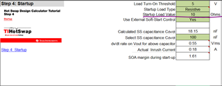
    and how to know startup load value???

  • Hi Lim,

    All of these values are system dependent and to be decided by you.'

    1. Over-current timer duration is the time for which excessive current is acceptable.

    2. Maximum allowed inrush current is your system decision.

    3. Current limit has to be more than 2.6A, you can choose to keep it more than 2,6A and less than short circuit limit.

    4. You can keep short circuit limit at around 1.5x/2x the over current limit. As far as there is no overlap in the ranges of cutoff.

    Regards,

    Shiven Dhir

  • thank you and i have a few question.

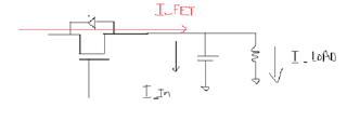
    1. can you explain difference between I_load and I_fet?

    actually, If I raise the value of C_dv/dt,  I_load  and I_fet become similar, and if i lower the value of C_dv/dt,  I_load  and I_fet  become different.

    2. how to decide the startup load value?

    3. If my system consumes 1A and the actual inrush current is 0.5A, is the total peak current generated 1.5A?

    4. What are the side effects if  Maximum allowed inrush current is too high?

  • Hi Lim,

    1. I_Load is the current in downstream load and I_fet is I_LOAD + INRUSH current.

    2. Startup load value is the amount of current that downstream load will consume after 5V (according to your calculator). 

    3. Yes.

    4. Higher Inrush means higher peak currents and can damage the board or MOSFET.

    Regards,

    Shiven Dhir

  • Thank you for answering my question.

    I have some more question.

    1. Does V_IMON just need to satisfy the range from 0V to 5V? is there any influence on V_IMON value?

    2. What is the effect if the C_dv/dt value becomes too large or too small?

    3.


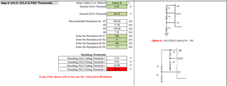
    I set it up like the picture above, but why does the red light come on?
  • Hi Lim,

    1. It needs to satisfy the range. Its influence depends on your needs. If you are using information from IMON to take system level decisions using an ADC or MCU as an example. 

    2. Cdv_dT decides the slew rate of output and HGATE ramp. It influences inrush current, turn-on time and MSOFET SOA.

    3. It is red because it at borderline. You can ignore the red color, it is fine.

    Regards,

    Shiven Dhir

  • HI shiven,

    I want to know a maximum Rg and dv/dt value.

    If turn on time is too large, what is happening?

    to be honest, i don't know that the longer turn on time , the worse system is

  • Hi Lim,

    You can keep Rg as 100ohms. dv/dt depends on your system requirements. You can start with 10nF.

    If turn-on time is higher, delay between VIN high and VOUT high will increase. Thats it

    Regards,

    Shiven Dhir