This thread has been locked.

If you have a related question, please click the "Ask a related question" button in the top right corner. The newly created question will be automatically linked to this question.

LM70660: Two layer layout example to be published?

Part Number: LM70660

Tool/software:

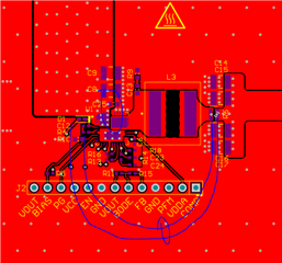
In section 7.4.2 in the LM70660 only shows the top layer of the layout example and I wanted to ask two things

1) Are there any intentions of adding another figure that shows the bottom side of that layout example board?

2) Is it possible to show how to ideally layout the passive components with a two-layer board?

I ask this to minimize the number of revisions that are bound to happen with the PCB design that I'm currently working on with the LM70660

  • Hi Christopher,

    We are not intending to update the layout example, but, you can refer to the layer plots contained in the EVM user's guide.

    This layout could also serve as a basis for a 2lyr layout as the majority of routing was done in the top layer. The bottom layer underneath the IC should be reserved for ground. Also if you want to proceed with 2lyr board, this is where I would route the current sense.

    Luckily, with the pin layout, you can route the current sense in the bottom layer where it won't interrupt the power stage return.

    Please feel free to post with your first pass layout for review.