Other Parts Discussed in Thread: BQ25713, TPS65988
Tool/software:
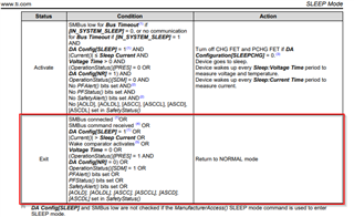
Hi, I am designing a powerbank (4s2p) that must support OTG and I have chosen the BQ40Z50-R2 as the BMS IC. I wanted to implement a form of low power mode as I can see the input voltage can go as low as 2 V. Therefore, instead of powering the BMS with the entire battery stack and consume more power, I wanted to use either a LDO or low power switch mode to lower the input supply voltage to e.g. 3.3V. However, as I understand the datasheet, the primary power supply input pin BAT and secondary power supply input pin VCC must be within 2.2 V of each other. This would mean that both VCC and BAT should be supplied from the output of either the LDO or switch mode. Assuming I can get the switching circuitry to work this way, is there any issues with this approach I am not aware in this text?
See the drawing for a visualization of what I want to achieve, and please ask if anything is uncertain, it was made slightly on-the-fly.

As a side question, even though I know it might be considered bad style, could an alternative to the above approach be to route the output power of the low power circuitry to the PBI pin?
Thanks in advance.
Kind regards, Victor