Because of the Thanksgiving holiday in the U.S., TI E2E™ design support forum responses may be delayed from November 25 through December 2. Thank you for your patience.

UCC28064A: Is switching expected at VINAC 0v points?

Part Number: UCC28064A

Tool/software:

Hi - I've got a PFC circuit running taking a 115V AC and generating 400V DC.  Target output is around 700W and I will be doubling the circuit up once everything is running sweetly to get 1.2kW+

At the moment I'm getting awful PF figures (of around 0.3 at no load, peaking at 0.7 at about 200W and dropping back to about 0.5 at 500W+)

Obviously the intention is a near-unity PF, so something isn't right.  Upon analysing the switching pulses, when the VINAC signal drops around 0V, the GDA and GDB outputs both stop switching and re-start again when VINAC rises on the next half-cycle.  The switching timing is fairly steady during the half-cycle when they are active and you can see it varying the on/off times as VINAC rises and falls.  (My test load is 100% resistive at the moment - a bunch of heater elements keeping my feet warm).

Should this stop-start be expected at the 0V points, or should the switching continue throughout the cycle?  At the moment they are off for about 20% of the time.  And significantly as the switches come back on, they start in-phase with each other and do not settle into interleaved mode until the waveform is at around the peak, so we are only running in interleaved mode for about 40-50% of the time.  Is that also to be expected?  That the two phases are in-phase to start with?

I've tried with/without the funky diode arrangement for low-VINAC distortion improvement.  With, no improvement.  I've also tried playing around with enabling and disabling both BRST and PHB trigger points.  All with no effect.
My inductors are currently 250uH, and I'm wondering if they are too small as I've had to increase switching freq (increasing RTSET) to prevent current walk-up.  But would too-small inductance here prevent the switching at low VINAC?  Would putting a 100uH in series with them be an easier/sensible solution rather than re-winding the custom magnetics?
  • Hello Tom, 

    Definitely something is not right, to get the results and behavior that you are getting. 

    Switching may or may not continue through the zero-crossing points, depending on the ZCD signals. 
    The next switching cycle is not automatic, it is triggered by the ZCD signal of the previous switching cycle.  

    ZCD (zero-current detection) is determined by two criteria:
    1. The voltage at the ZCDx input must exceed a 1.7V-threshold during the corresponding MOSFET's off-time (during the inductor demagnetization time), and
    2. That ZCDx voltage must then fall below a 1.0V-threshold at the end of demagnetization to trigger the next MOSFET turn-on.

    If the inductor turns-ratio is such that either of those voltage thresholds cannot be met, then no subsequent turn-on will happen and the switching stops (in that phase). 
    Since the two phases are likely to have nearly identical properties, it is highly probable that both phases stop switching about the same time.
    Once ZCDx is lost, it cannot be regenerated spontaneously.  It needs some other pulse source to restart switching. 

    A built-in "watch-dog" timer delivers a restart pulse to both phases every ~210us if either one of them loses ZCD.  This timer is reset when both ZCDx signals are firing, or ZCDA alone if Phase-B is shut down by PHB, so it doesn't interfere with normal running. 

    The two phases will always restart in-phase, but should migrate to out of phase operation within several switching pulses. 
    They also start in-phase each cycle if OCP is triggered at the CS input (see datasheet).  But that (OCP) doesn't make sense since OCP usually occurs near the peak of the line current, not along the "walls".  Check to see if the in-phase switching occurs at ~210us period.  If so, then the ZCDx signals are not in spec to sustain switching until the input voltage has risen to some level. 
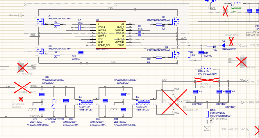
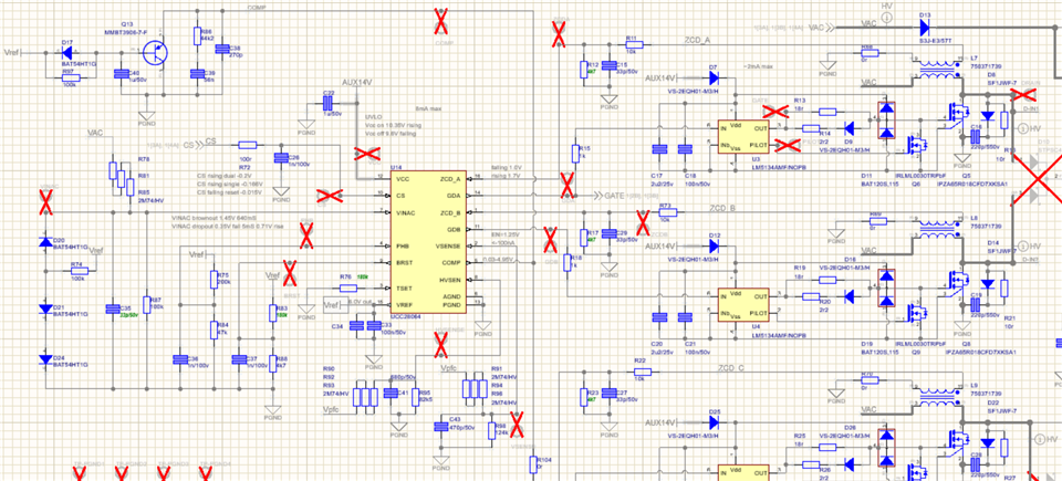
    The resistor dividers on ZCDx (R11 and R12 for example) are unusual, and may contribute to the problem. 
    Also, I recommend to set R11 to at least 20kR, to avoid excess current into and/or out of the ZCD input.   

    250uH does not sound like "too small" of an inductance.  However, there is no information about the ZCD-winding turns ratio, so that must be checked.  
    Generally, if the PFC design is done using the UCC28064A Excel calculator tool, then it should work correctly (barring assembly error or extremely bad pcb layout). 
    https://dr-download.ti.com/design-tools-simulation/calculation-tool/MD-0YHPu8SvFB/01.00.00.0C/sluc645c.zip 

    Regards,
    Ulrich

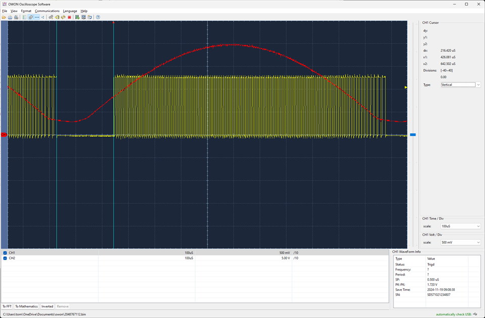
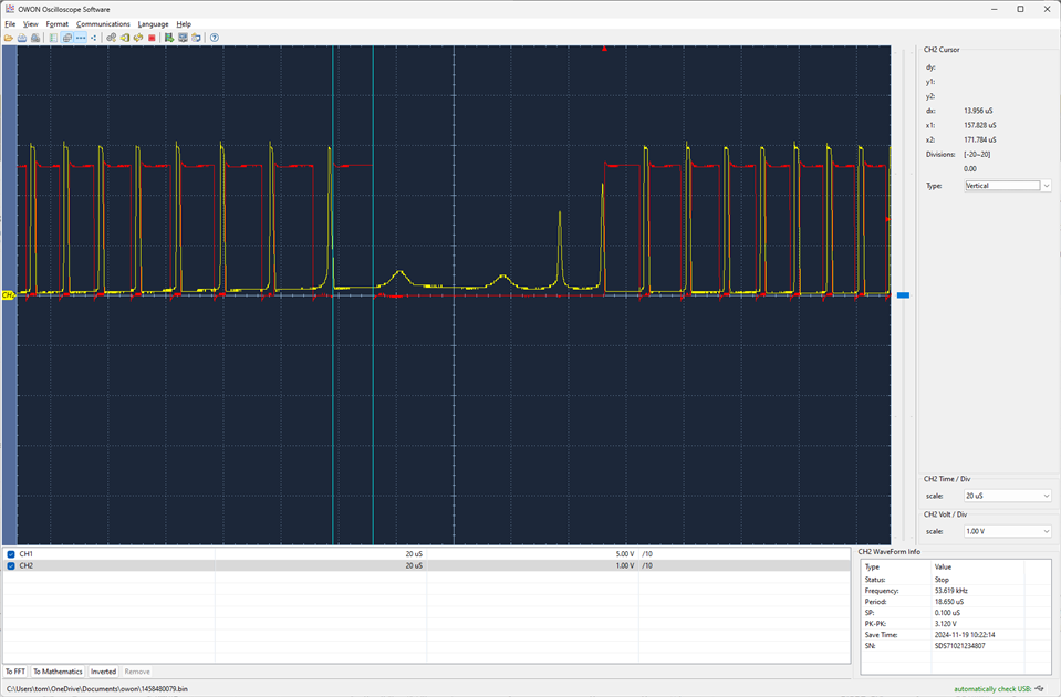
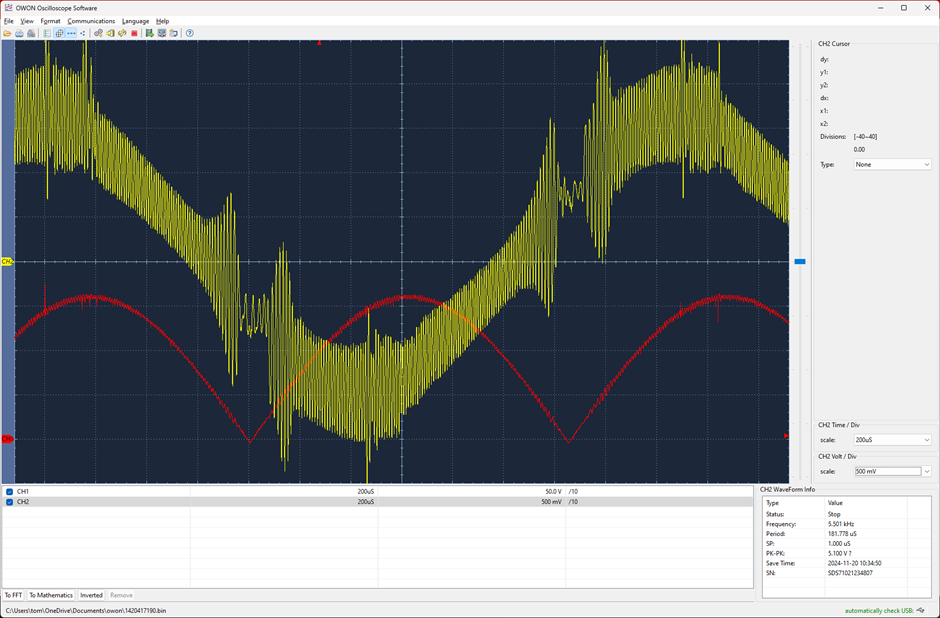
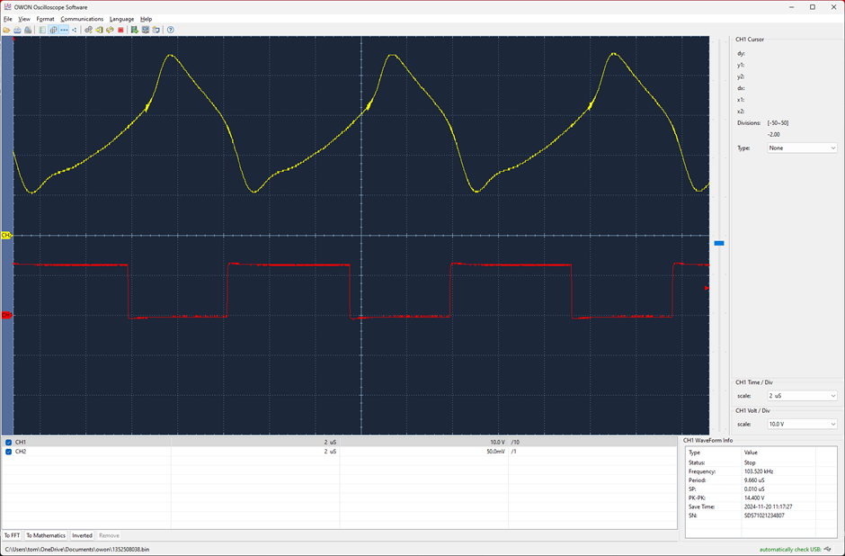
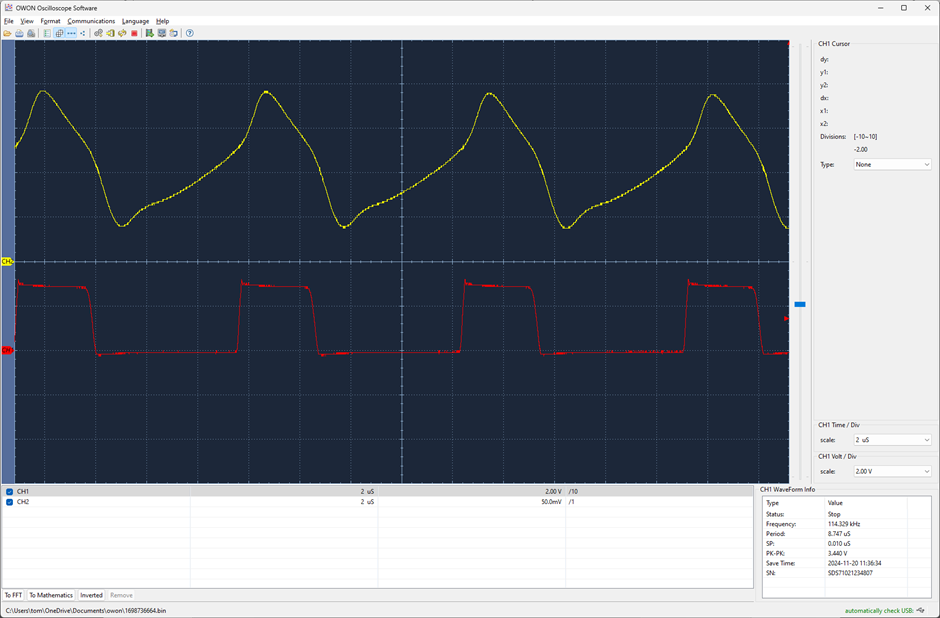
  • Thanks, Ulrich - I thought I'd come back with some plots to visualise the issue.  First off this is VINAC (red) and GDA (yellow).  As per your suggestion above, the off-period is 217uS, which would indicate your suspicion that it's something to do with the VCD.

    (by the way, my AC source is 400Hz, so 800Hz rectified - as this is an aerospace development)

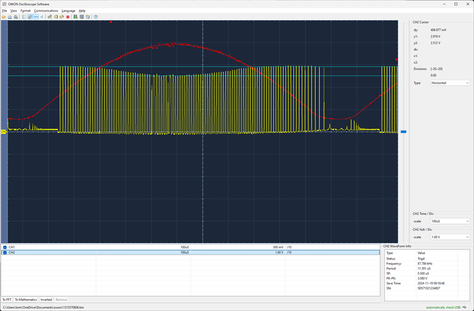
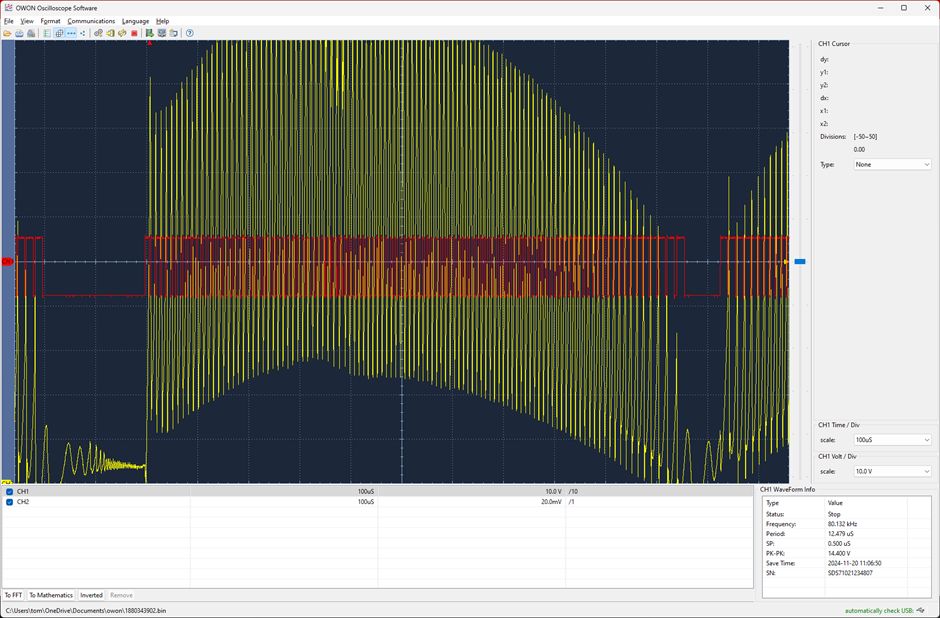
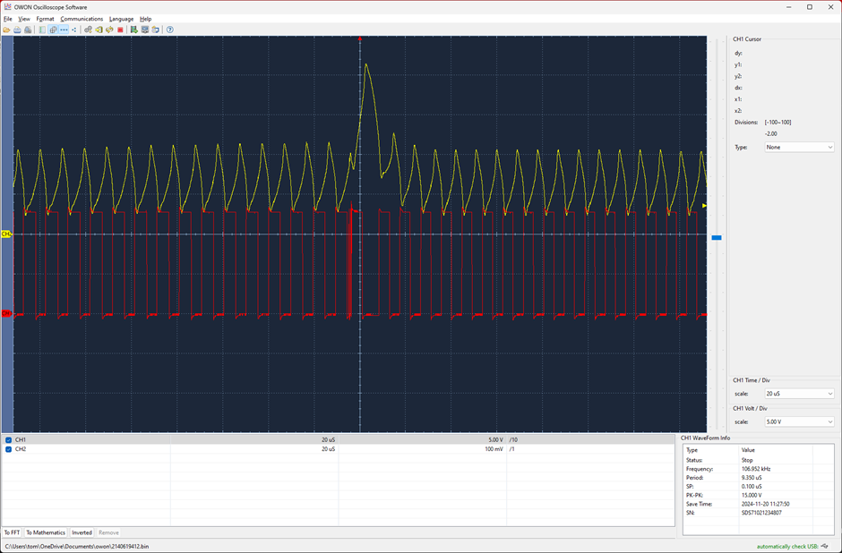
    This next one is ZCDA and VINAC.  ZCDA is at 1V/div so the higher peaks are around 3V and it dips to 2.5ish at the peak of VINAC.  I do see some tiny 0.5V spikes during the down time.  The last successful spike before switching stops is only just shy of 3V, so I can't see why it then suddenly decides to stop switching.

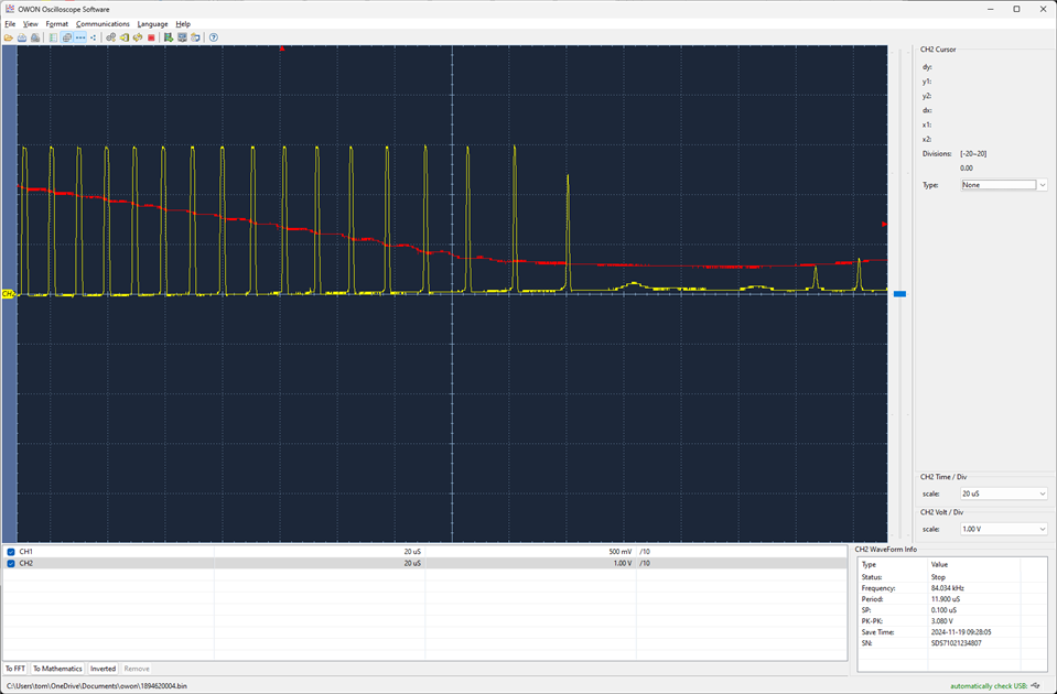
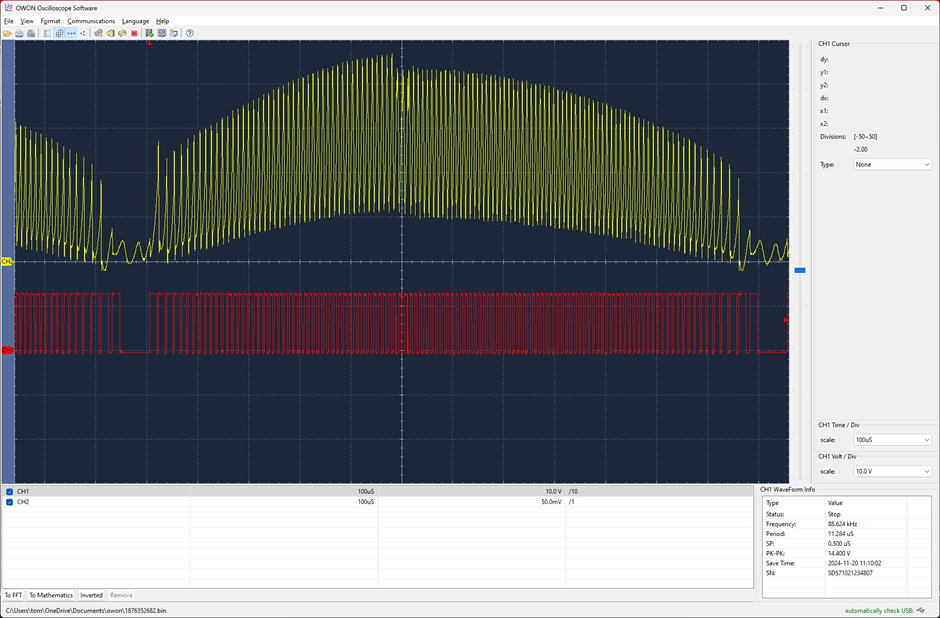
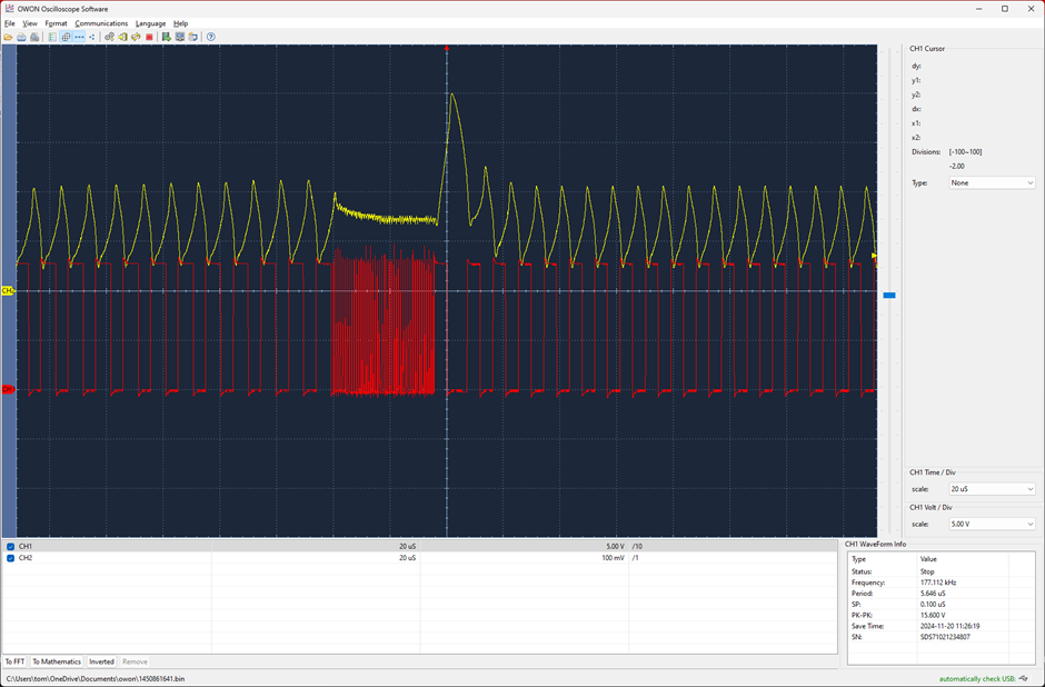
    Here is a close up of the end of the cycle...

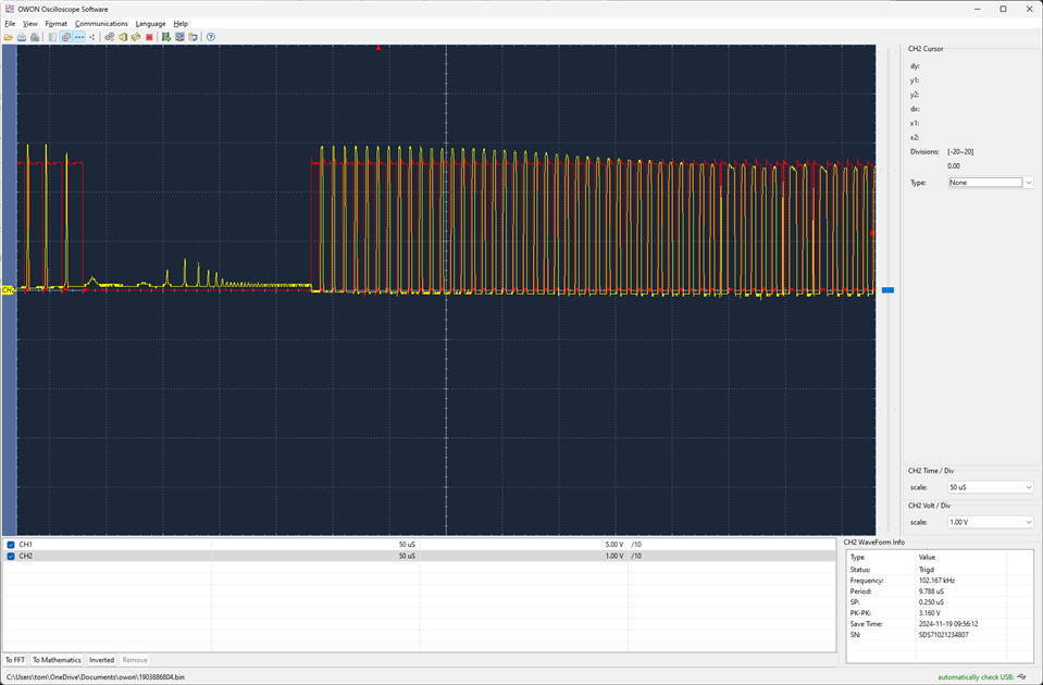
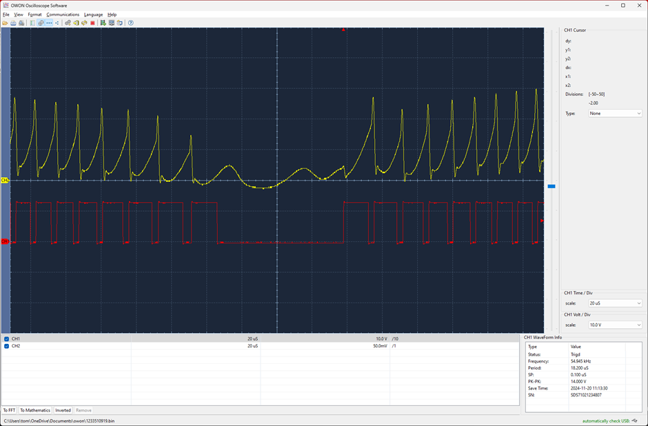
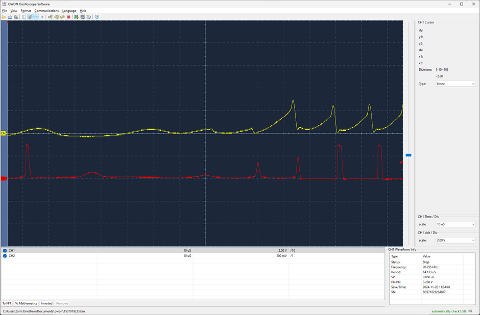
    And a focus on the GDA (red) with ZCDA (yellow)...

    And this is showing that the last GDA switch on/off, is not followed by a ZCDA pulse - which I guess is our problem.  So I'll play with that resistor value...

    Removing the pull down resistor and cap and changing the series resistor to 20k...

    We see an improvement - it jitters a fair bit, but generally the down-time is now around 80uS.  This now would indicate it's now not the 210uS watchdog which is waking it up.  My ZCD transformer is 250uH, 32:1 ratio.  Revisiting the maths, we should be looking at 385uH and 100:1 ratio - but a higher ratio would just result in smaller ZCDA pulses.  Because of the lower inductance, I've had to speed up my switching - so are we now hitting a maximum on-time limit somewhere?
    What are these small pulses on the ZCDA signal above which are not related to a switching from GDA?

    My PF is still really bad - and if I look at the current coming in on the AC, it's really noisy.  Any other thoughts?

  • Hello Tom, 

    Thank you for the waveforms; they help quite a bit. 
    I think we'll need to examine additional waveforms to put some quantity into your qualitative comments: 
    "...PF is still really bad...", "... it jitters a fair bit...", "...getting awful PF figures...", etc. 

    Specifically, I'd like to see:
    1. a half-cycle of the AC input current with respect to the rectified input voltage (100us/div sweep),
    2. a half-line cycle of Phase-A inductor current, amplitude maximized to the scope vertical window = 1A/div, along with GDA at 10V/div, 100us/div.  
    3. a few zoom-ins of #2 plus ZCDA (2V/div) at beginning, peak, and end of half-cycle, at 10us/div. 

    Also, I'd like to know the full range of your input voltage requirement. 115Vac +/-?,  360Hz~800Hz?   Actual Pout max (per controller)?  
    What size is your Cout?   What values do you have for Cin and your EMI-filter X-caps? 

    The boost MOSFET in your schematic diagram is massive.  I think it is much too big for this application. Coss when ON gets up to 100,000pF!
    This Coss accounts for the little bumps (pulses) on the ZCD signal during the non-switching time.  It is reflected voltage of the boost inductance resonating with the massive Coss while the FET is off, but there is still a little input voltage near the zero-cross. 
    Since this Coss is highly non-linear, it drops greatly as Vds rises, and the inductor resonant current drives Vds high enough to reflect to > 1.7V on the ZCDA and actually restarts switching in Phase-A without needing the internal restart timer!  I assume that Phase-B does something similar. 

    Anyway, a much smaller FET may be in order, to reduce the turn-off delay that I see occurring and which interferes with proper PFC control. 
    Some quick numbers for context: 
    700W / 2-phases = 350W / 0.93 = 376W / 115Vrms = 3.27Arms = 4.63Apk => 9.26Apk inductor current at peak of input voltage.  
    Per equation (39) in the datasheet, Ids(rms) = 0.451Arms in a FET with 18mR resistance = 3.7mW conduction loss. 
    I think you can easily reduce your MOSFET size by a factor of 10, but I recommend even more to greatly reduce Coss and its contribution to switching loss. 

    I have not done the math yet, but I think your 250uH inductance is okay, does not need increasing.  The turns-ratio could actually be decreased, not increased above 32:1.   

    But before making a lot of changes, let's see what you get for waveforms. 
    Please include the test conditions for each screen-capture. 
    And please don't forget to provide the other information that I requested. 

    Regards,
    Ulrich

  • Again, thank you Ulrich for taking time to look at this for me.  I have to admit, your support is invaluable.
    Let's see if I've covered everything you've asked...


    Input filter and active rectifier.


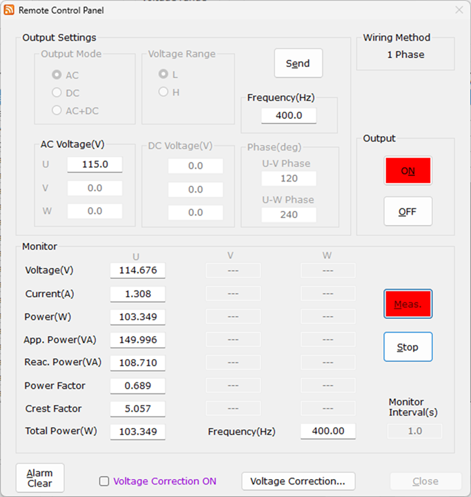
    This is the AC source supply monitor.  Test conditions are, 115V, 400Hz, AC in, through the AC filtering, through the active rectifier and into the PFC stage.  Output of PFC stage is running into a 1.6k resistor giving us a 100W load.

    As you can see above, the supply is indicating a PF of 0.689.  This gets worse at around 200W load (0.5), better at 300W (0.87) and bad again at 400W (0.52) - I can't easily get more granular than 100W increments without re-wiring my resistive load, and my digital load is only rated to 150V.

    Target design is a civil aerospace power supply, so 115V (97-134), 400Hz (360-800).  Output power is 1200W, DC and I have 2x 28064 working together, so each needs to be able to do 600W with each phase doing 300W.
    My Cout is currently 240uF, although there is space on the dev board for another cap to take it to 480uF.  There's also a few x 10nF of high-frequency decoupling on the PFC output.


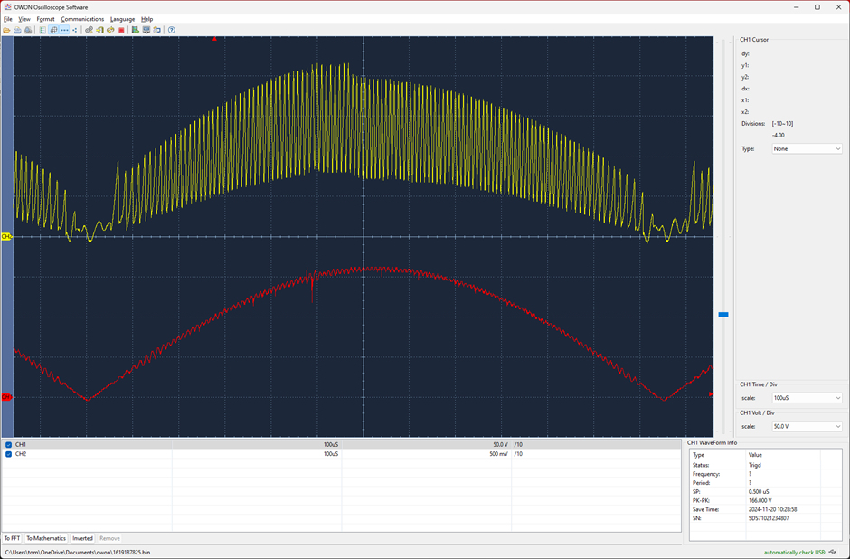
    Plot-1.  VAC (rectifier output) current (y) and voltage (r).


    Plot-2.  This is the AC input current relative to VAC


    Plot-3a


    Plot-3b.  Both 3a and 3b show the primary inductor current (y) and GDA (r)


    Plot-4.  Close-up of the zero-V point showing primary inductor and GDA


    Plot-5.  Focus in on the 1st pulse of a new cycle.


    Plot-6.  Focus in on a pulse about 400us into a cycle (roughly mid cycle)


    Plot-7. An occasional glitch, mid cycle seems to cause a double-ON which leads to a big current spike in the inductor.  (See video below)


    Plot-8 - and every now and then that glitch seems to be worse and the GDA signal goes into some kind of oscillation.  This always occurs at the same point in the half-cycle. (See video below)


    Plot-9.  Showing primary current (y) and ZCDA (r) - focus at 0V point of cycle


    Plot-10.  As above but at mid-cycle.

    Video of 'glitch':   20241120_113301.mp4 https://1drv.ms/v/s!AmJSDsbcxXMBnNd5sbVo0TmfG9lVvA?e=GXavF7


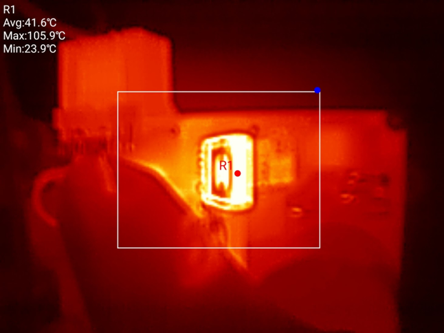
    And just for interest - thermal image shows FET is running at about 106 degrees in free air.  Single phase operation at the moment - so this chap is doing all the work.

    I note your comments about my FET over-kill choice.  I'll see what else I've got in the parts bin and try something a little smaller to see what happens.

  • Hello Tom, 

    Thank you for the profuse waveforms, they help a lot.  And the additional schematic.  

    Let me get the easy part out of the way, first.  A lot of your poor PF comes from the X-caps in your line filter, including the caps across the output of the bridge rectifier.  Summing this capacitance comes to about 5 x 330nF = 1.65uF at 115Vrms at 400Hz:  Ixcap = 115V/Xc = 115V x 2*pi*400Hz*1.65uF = 0.477Arms.

    An ideal 100W load at 0.95 efficiency at PF = 1 would have Iac = 100W / 0.95 / 115Vrms = 0.915Arms. 
    So at ~100W load, the X-cap reactive input current is more than 1/2 of the real power current.  Note that this will get twice as bad at 800Hz input.  
    The semi-good news is that higher real load power will reduce the reactive portion of the input VA and PF should always get higher as load power rises. 
    The X-cap current will never get higher (other than at max Vin of 134Vrms) than what it is at 800Hz.   

    The bad news is that X-cap reactive current is only part of the low PF you are getting. The other substantial part of low PF is high harmonic distortion, which can be seen by the high frequency content of the input current seen in Plot 2. (Plot 2 also shows the phase shift due to the X-cap current.)
    And since your PF was seen to get worse, then better, then worse again as you increased your load, it indicates that greatly varying THDi has the major influence on the PF, since the X-cap current stays constant. 

    Now to analyze the current waveforms: 
    1.  The current scale is listed in mV/div, so I'm guessing that Plot 1 equivalent scale is 0.5A/div based on 100W load.  I don't know if the other plots are all at the same scale. (In future plots, please indicate actual scaling.)
    2.  Plot 1 shows output current of bridge rectifier which is the sum of the two inductor currents of the interleaved phases. (I assume 2-phase operation despite your comment about running single-phase for the thermal image. Please correct me if my assumption is wrong.)  
    3.  Plot 2 shows the AC input current still has substantial high-freq content, so I think the EMI filter is not doing a very good job. I think you may need quite a bit more differential mode inductance to relieve the burden on X-caps for DM, since you may want to reduce total X-cap to improve PF even at full power, once all the distortion is gone.   
    4.  If Plot 3a and 3b are really of one inductor current, then the bottom envelope of the ripple current in 3b indicates the presents of CCM in the inductor. 
    5.  However, close-ups of the ripple currents have strange shapes, so I am not sure that I can totally believe the waveform in 3b. 
    6.  Plot 4 shows the expected rising inductor current during the GDA on-time, except that closer looks shows that the current continues to rise after GDA goes low.  Even that can be expected due to the long turn-off delay from the massive Coss of the MOSFEY, but the current goes an peaks up even higher, faster when the next GDA pulse comes along.  This peaking resembles saturation of the core. 
    7.  But then, Plot 5 and especially plot 6 does not look right at all.  In Plot 6, inductor current rises a full microsecond into the off time (which could be from the Coss) but then falls and then falls even faster after the next cycle GDA goes high.  That does not make sense, and makes me doubt the accuracy of your current measurements.  Not the overall waveshape (high freq riding on low freq), but the details of each switching cycle. 
    8.  The glitch in plot 7 may be due to a noise glitch on ZCDA that prematurely triggers a new cycle before the previous one had finished demagnetizing. 
    9.  The "glitch" in Plot 8 is really weird, and I've never seen that behavior.  I don't know how to explain it except to guess that it started with noise that generated additional noise which then self-sustains to rapidly retrigger itself for an interval of time until conditions change enough to halt the oscillation.  
    10.  I don't have much to say about plots 9 & 10. 
    11.  I am not able to view the video, since TI's security blocks access to an unsecure link or unverifiable file. 

    What kind of current probe are you using?  Does it have the bandwidth for >150kHz signal (certainly with >1MHz harmonic content)?

    Despite the work that you put into this (which I do appreciate) I doubt the veracity of the current shapes. I think the probe you used distorts them somehow and I don't want to draw conclusions from inaccurate data.  If you can prove that they are 100% correct, then that is some weird inductance you have there. 

    What kind of core material are you using, by the way?

    As for the thermal image, it looks like you have no heatsink on that FET.  I suggest to clip a piece of metal to it and/or blow some air on it to cool it off, so it doesn't blow up on you and possibly take out some other parts of the circuit with it.
    Most of the losses in there are switching losses from the Eoss curve (Diagram 15 in the IPZA65R018CFD7 datasheet) ~32uJ at 150kHz = 4.8W.

    Progressively smaller FETs will drop the Eoss losses faster than the Rds(on) losses increase until you come to a FET where conduction losses are approximately equal to switching losses.  That's the point to stop if you always run at full power. B ut Fsw goes up at light loads and Rds loss goes down, so if higher efficiency at lighter load is required, then continue reducing FET size for higher Rds(on) and lower Coss (Eoss) until you reach the equality point at the lighter load of interest. 
    Note: you do not need a FET with ultra-fast body diode (CFD7 suffix) for this application.  A C7 or P7 device (or equivalent) will work fine. 

    Regards,
    Ulrich