Tool/software:
Tool/software:


Hey,
Thank you for reaching out to TI with your questions regarding the UCC27537.
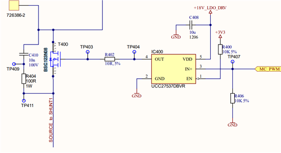
With regards to the schematic, I have a couple of suggestions.
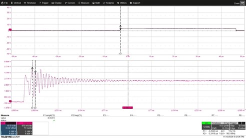
1. We recommend placing an RC filter on the input pins placed closed to the gate driver. Typical ranges for the components are 0-100 Ohms and 10-100pF. This will help with the noise that is seen from the MCU on the input.
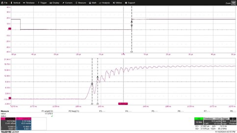
2. For the ripple seen on the output, this is largely a result of the noise on the input as the driver is receiving mixed signals due to that input noise.
3. Please ensure that C408 is placed as close to the driver as possible. You could also add a 100nF in parallel to C408 beside the driver for transient response.
4. Adjusting the gate resistance R402 will also affect the rising and falling edges of the output by limiting output current.
5. For EN enable, this could also be connected to the 18V supply rail as well.
6. Layout is also important for noise. The gate drive path to the MOSFET should be as short as possible and have a wide trace. The high current paths such as VDD and GND should also have wide traces.
Let me know if there are any further questions.
Thank you,
William Moore