Tool/software:
Hello,
a new design using LM74930-Q1 has the requirement, that the whole device stays fully operational during a 2ms power interrupt at supply voltage input (from ISO 11783-2, tractors and machinery for agriculture..).
To implement this feature, a buffer capacitor at the output of the LM74930-Q1 circuit will be used.
However, when dimensioning the required buffer capacitance, startup or reactivation delays of LM74930-Q1 have to be considered and added to the required 2ms interruption.
At the moment it is not clear to me which reactivation delay after the 2ms interruption will be present.
One hint is formula (1) in DS giving the initial gate driver enable delay:
![]()
With Cvcap=100nF and Vvcap_uvlor=6.6 --> Tdrv_en=419µs.
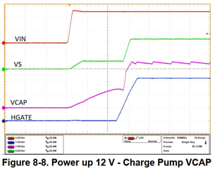
On the other side, figure 8-8 in DS shows a ~12ms delay between VIN rising and HGATE being ramped up.
The ramp up duration of HGATE signal is determined by external Cdvdt=10nF and HGATE source curren I(hgate)=55µA.

So the real power up delay in the example application is 15ms according to fig. 8-9.
This would lead to a much larger buffer capacitance needed in order to let the device stay fully operational during a 2ms power interrupt.
My questions are:
1) Is there a way of calculating the real power up delay (in example application it is 15ms according to fig. 8-9)?
2) What options are there for reducing the reactivation time after the 2ms power interrupt? For example, would it be possible to let the LM74930-Q1 stay alive by using a larger capacitor value Cvs at VS input of the LM74930-Q1?
Thanks in advance.

