This thread has been locked.

If you have a related question, please click the "Ask a related question" button in the top right corner. The newly created question will be automatically linked to this question.

TPS40210: What is the difference between catalog and automotive version?

Part Number: TPS40210


Tool/software:

Hello,

I have a question regarding TPS40210 family's DC-DC ICs.

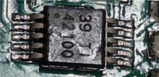
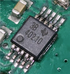
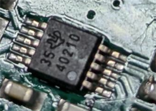
Main question is what's difference between TPS40210 catalog version (TPS40210DGQ) and automotive version (TPS40210QDGQRQ1)? Because previously we were using catalog version and everything was working fine and then we replaced it by automotive version.

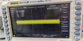
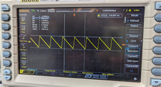
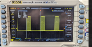
Since we replaced to TPS40210QDGQRQ1 automotive version, the dcdc was unstable under the load, its constantly resetting, similar to overcurrent state but when the load is disconnected the dcdc works normally.

The main problem was that DIS/EN pin was left floating but according the datasheet, the dcdc has 1Mohm pulldown to GND which should be okay for normal operation. We tried to pulldown directly DIS/EN pin to GND and the dcdc started work normally.

So, my question is what's the difference between these two dcdcs and why one's working normally without external pulldown and another requires external to work normal.

Maybe there is some possibilities that the automotive version have more noise and internal 1Mohm pulldown is not enough.

Best regards,

  • Hi Egidijus,

    Thanks for using the e2e forum.
    From functional side, there should be no differences between catalog and automotive version. They have the same features and should behave identical within the recommended operation conditions.
    However, the TPS40210-Q1 version recently got reworked and upgraded to a new fabrication process. The datasheet and all specs stayed the same, but the internal structure changed. It could be possible that your timing of switching the devices matched with our device replacement.

    As said, the behavior should not be different during normal operation conditions, but it could be the case the new device reacts different to noise interference.
    As the old device mentions a 1MOhm resistor from DIS/EN to GND, this is also implemented in the new version.

    My guess would be that there is some noise injecting into this high impedance DIS/EN pin which may cause ringing on the signal and enables/disables the device over and over.
    I would strongly recommend to add an external connection from DIS/EN to GND to remove the high noise sensitivity and stabilize the controller (independent of which device version is used).

    Best regards,
    Niklas

  • Hello,

    I've tried to connect DIS/EN directly to the GND plane of dcdc plane, but nothing changed, but I noticed that if I touch with tweezers the GND of the capacitor or somewhere else in this GND plane, the dcdc starts working. 

    A bit about my circuit: the circuit is very similar to the reference design by components parameters but has in the output 32v voltage, but in my opinion that output voltage isn't make a lot difference to not work circuit properly. Main difference is that output of the dcdc is connected to the common mode choke and connected to the main GND plane.

    I tried to connect 100nF capacitor between these two GND planes and circuit starts working. By any chance the noise in dcdc GND plane is so big that this dcdc is not capable to start working and any added capacitance decreases noice?

    Best regards, 

  • Hello Egidijus,

    Thanks for the quick feedback.

    Would it be possible share the schematic and layout of the TPS40210 design? (Even if its close to the EVM, there might still be differences)
    Then I can review the design and check for possible root causes.

    Thanks and best regards,
    Niklas

  • Hello Niklas,

    Sorry for a late reply, I did not have an opportunity to snap some screenshots of the circuit.

    In the pictures below you can see circuit diagram and PCB layout. All tracing is on TOP layer, MOSFET control is via trace in INEAR layer and current shunt resistor voltage sensing is as well in INEAR layer. If it's would be needed I can also upload here. The GND plane in only on TOP layer, as I can see there are some vias but these vias are not connected to the bottom layer... (TOP layer - RED, BOTTOM layer - BLUE).


    Best regards,

  • Hello Egidijus,

    Thanks for sharing the files.
    The layout shows there is no separation of analog and power ground. The IC circuit put on the right side away from the power stage, which is not bad, but the main output current still flows through the choke which is close the the IC components.

    The fact that you can influence the operation of the controller just by touching the ground plane with tweezers indicates this is indeed a noise issue.

    Another thing I noticed within the layout is that the full output power has to flow through the small path below the sense resistor as the +32V_in plane becomes narrow and widens again. However, I cannot tell if this contributes to the noise as well.

    I tried to connect 100nF capacitor between these two GND planes and circuit starts working. By any chance the noise in dcdc GND plane is so big that this dcdc is not capable to start working and any added capacitance decreases noice?


    This could indeed be possible. It is common to place caps between isolated GND caps to help shunt common-mode switching noise current from the output side of a transformer or choke back to the input side.

    Best regards,
    Niklas

  • Hello Niklas,

    Sorry for a late reply.

    I was trying to figure out why TPS40210 is not working properly. I thought that the main problem is DIS/EN pin but in reality when i started to measure output voltage with oscilloscope, I found that TPS40210 catalog version works differently from the automotive version.

    Then I bought another 30 catalog version ICs with part no.: TPS40210DGQ, TPS40210DGQRG4, TPS40210DGQR. Every mentioned IC have same marking number but different i think date code or something. In the tests i found  that only TPS40210DGQ works in my design, the code was "35".

    Then I captured some oscilloscope photos of good working IC and bad working IC:


    Voltage ripple before common mode choke of "good" IC:

    Voltage ripple after common mode choke of "good" IC:


    Voltage ripple before common mode choke of "bad" IC:


    Voltage ripple after common mode choke of "bad" IC:


    Then, i tried to measure PWM on the gate of the mosfet. I found that PWM is not generated constantly as it should but IC generated PWM by some period of time and I think there is the the main reason why i saw in output saw type of voltage signal.


    May you have some ideas why automotive version and other catalog version skips pulses and makes in the output saw type signal?

  • Hello Egidijus,

    Thanks for the update and further testing.

    If the issue is not related to enable/disable, but to the light load switching behavior of the device, there is one difference between the previous material and the new device version.
    When the load is small and the device duty cycle of the TPS40210 is close to the minimum on-time restriction of the device, the device will enter pulse skip mode to avoid a runaway of the output voltage.
    While the previous device could send out single pulses with flexible delay time within each pulse, the new version will burst out several pulses and then wait for a longer time. This may affect the EMI behavior of the device.

    If you increase the load on the application, both old and new device should enter PWM operation with fixed switching frequency, where they should behave the same again.

    Could you give me the markings/date codes of the ICs that are working and that are not working in your application?
    Based on this I can find out which is the original and the new IC version material.

    Best regards,
    Niklas

  • Hello Niklas,

    I want to correct you that the problem occurs not only at light loads but and also at higher ones. Today i tried to modify current sense circuit but there was no effect. Previous components was Ccomp = 2.2nF, Rcomp = 18.7kOhm, Ch = 47pF. Then I tried to modify compensation loop components to Ccomp = 100nF, Rcomp = 11kOhm, Ch = 10pF and whole circuit starts working, also voltage ripple drastically decreases.

    So I was confused why using the TPS40210 's calculator's components values was completely different from these (Ccomp = 100nF, Rcomp = 11kOhm, Ch = 10pF). Because if I solder components with values of calculator, the circuit not works.

    After that, I tried to solder these components (Ccomp = 100nF, Rcomp = 11kOhm, Ch = 10pF) to the working PCB with date code (35). There was no difference. So the main question why the circuits works completely different with the same layout, same part marking and even same components.

    Not working part markings:


    Working part markings:


    Best regards,


  • Hello Egidijus,

    we will check that and reply within the next day.

    regards 
    Johannes

  • Hello Egidijus,

    Sorry for the long delay. I was out for the last days and returned today to the office.

    According to the date codes on the ICs, all 'bad' ICs are from the second half of 2023, where the rework of the device is already implemented in the market.
    The 'good' ICs all have older date codes and should therefore be the old device material.

    Unfortunately, it is not possible to request a supply of the old material exclusively, as the old material will slowly fade out to get fully replaced.
    The best solution would be to optimize the board design to achieve acceptable results with the new material.

    You mentioned the behavior is also different at higher loads. What is the point of load when the system stabilizes? (Or is it not stable even at max load condition?)
    There are also some additional improvement on top of the previous layout comments so far:
    - The output caps are only rated for 35V. This leaves very small margin. Higher rated caps should be better here (e.g. 50V rating)
    - Ceramic caps are much better at filtering switching noise due to lower ESR than bulk capacitors. We recommend to add some additional ceramic capacitance
    - Can you also show where the feedback signal trace is located? Is is close to the diode or close to the capacitors? (There are no inner layers shown in the picture). It is recommended to place the feedback trace close to the caps to reduce noise.

    Best regards,
    Niklas