Because of the Thanksgiving holiday in the U.S., TI E2E™ design support forum responses may be delayed from November 25 through December 2. Thank you for your patience.

UCC28064A: How to set peak current limit and on-time in single mode

Part Number: UCC28064A

Tool/software:

Hello.

To allow the UCC28064A to operate in continuous single-phase mode, the PHB input was connected to VREF to disable phase B operation. Also, the coil is disconnected and the ZCDB signal is not generating anything. Although it is operating in single mode, I have two questions.

The first is that the peak current limit threshold on the CS pin input has not changed from dual mode (0.2V) to single mode (0.166V). I am aware that the threshold is 0.2V at startup and the threshold changes to 0.166V after 14 line half-cycles of Vinac.
On the current board, the current detection resistor is 12mΩ and the peak current is calculated to be 16.6A (at startup)/13.8A (at steady state), but when I operate the board on the actual device, the peak current is 16.6A at both startup and steady state. Is there any way to resolve this?

Second, I would like to know how to determine the optimal Rtset in single mode.

thanks.

  • Hello Yasuda-san, 

    I am not sure how to explain having the same peak current at both start-up and steady-state while in single-phase mode. 
    One possibility is that there is a large R-C filter on the CS pin and the time delay of the filter allows the peak current to rise to actual 16.6A before the CS input sees the apparent 13.8A level. 

    For optimal Rtest, I suggest this method: 
    In the usual 2-phase operation, Rtset programs the maximum on-time allowed for maximum load at minimum line voltage. The COMP voltage is presumed to be set at its maximum limit for the maximum power output.  Single-phase mode is intended be entered at a load level less than 1/2 of maximum load.  At half-load, each of 2 phases carries 1/4-load and COMP voltage sets the appropriate on-time (which is less than the maximum on-time).  Due to line feed-forward, Vcomp at 1/2 power is about 1/2 of Vcomp at max power. 

    When changing to single-phase mode, the 1/4-load of Phase-B must be assumed by Phase-A so its current must double. The input voltage is assumed not to change.  So when 1-phase mode is entered, Phase-A on-time is automatically doubled to allow Phase-A current to double with out disturbing the COMP voltage or causing significant Vout transient deviations. 

    Now, if single-phase mode is intended to carry the maximum load at minimum line, then it can be presumed that 2-Phase mode would normally carry twice that maximum load power, if there were two phases running.  But we want the COMP voltage to be at its maximum level at max power while in 1-phase mode, so since the on-time is doubled while in 1-phase mode, then 1/2 of that time would correspond to 2-phase mode with 1/2 power in each phase.  Therefore max power in one phase corresponds to "doubled" on-time when in 2-phase mode at the max power level.  

    Basically, I think that Rtset is chosen to be the value needed for 2-phase operation at 2X the maximum output power.  

    Consider it another way: 
    PHB voltage is set to 0V to force 2-phase interleaving. 
    Vcomp is maximum (~5V) at max power at minimum line and Rtset sets the maximum on-time necessary to deliver the power through 2 phases at regulated Vout.
    Load drops to 1/2 max power and Vcomp drops to ~2.5V so that on-time is cut in half in each phase. Each phase is delivering 1/4 of max power. 
    PHB voltage is raised above Vcomp, so operation changes to 1-phase mode and on-time doubles.  1-phase delivers 1/2 of max power at the original max on-time but Vcomp is still ~2.5V.  
    PHB is raised to 6V so 2-phase operation is no longer possible.  
    Load power is increased back to max power, so Vcomp must rise back to ~5V so that on-time can increase to 2X the original max on-time. 
    This requires Rtset to be chosen for 2-phase operation at double the maximum power. 

    Regards,
    Ulrich

  • Thanks for the answer. Ulrich-san.

    I will take your advice on how to design the Rtset.

    Regarding the peak current. I reduced the RC filter on the CS terminal as you suggested, but it didn't improve the spikes. So I'm trying to get to the root of the problem.
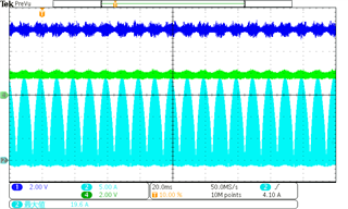
    Please see attached waveform 1. [Ch1: VPHB, Ch2: IL, Ch4: VCOMP] Notice that the VCOMP is smaller relative to the VPHB. Since this is the waveform when the IC is moved for a short while in steady state, the IC recognizes it as single mode and the peak current should be 13.8A (ROCP: 12mΩ, peak current limit threshold: 0.166V), but the peak current at this time is 16.6A (ROCP: 12mΩ, peak current limit threshold: 0.2V ). Reading from the datasheet, we think this should be the threshold for single mode. But I haven't been able to change the threshold from dual mode to single mode so far.
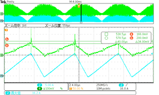
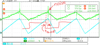
    Look at waveform 2. [Ch2: IL, Ch4: VCS] This is looking at the CS pin under the same conditions as waveform 1, but the spike voltage is so large that it is hard to see, but it is impossible to determine whether the threshold is 0.166V or 0.2V.

    Currently, the coil of phase B is removed and PHB is connected to Vref and Rtset is changed to 180kΩ which is calculated. Also, the IC has been replaced once and it has been confirmed that the IC is not defective. Is there any other means to set the threshold to single mode other than this? Also, is this situation where the threshold value at startup and the threshold value at steady state do not change normal, or will there be any problems in the future if we continue with this design?

    thanks.

    Waveform 1

    Waveform 2

  • Hello Yasuda-san,

    Thank you for the waveforms.  I think that waveform 2 makes things clearer for me. 

    First, the spikes in the green trace (Vcs) are just noise coupled into the voltage probe during the turn-off dv/dt of the MOSFET. 
    This noise can be reduced or even eliminated, by using the "tip & barrel" probing technique.
    See this App-note for clear photos of the method: https://www.analog.com/en/resources/app-notes/an-1144.html

    Second, I think the single-phase mode current threshold is actually at or close to -166mV, but there are a few time delays that add up before the MOSFET drain current actually stops rising:
    1.  CS threshold may be a little higher than -166mV due to tolerance.
    2.  CS input to GDA output time delay = 60ns (typ), 100ns (max) when measured with 50mV overdrive. 

    3.  Time delay from GDA beginning to fall to MOSFET Vgs threshold of the drain current to begin cutting off the channel.
    4.  Time delay from MOSFET channel cut-off to charge-up of Coss where Vds starts to rise quickly.

    To check this, please probe a third channel on you oscilloscope to view the GDA signal and look at the timing from GDA falling edge to peak of inductor current.  You can also compare the GDA falling edge to the rising voltage on Vcs (use 50mV/div and 1us/div for better resolution).

    GDA falling should be triggered by Vcs rising through the 166mV threshold about 60ns earlier in the waveform.  (It may not be exactly 166mV or exactly 60ns delay due to tolerances.)
    The noise spikes do not interfere with this threshold because the spikes occur well after the peak limit threshold is crossed. 
    Even so, tip & barrel probing will clean up the waveform so the important characteristics of the signal are not obscured. 

    There is no other way to achieve 1-phase mode other than setting PHB = 6V.  
    Assuming that your investigations verify what I suspect is happening (above), there should be no problem with your design operating this way.
    If the actual peak current limit must be at 13.8A, then I suggest to increase Rcs a little to account for the total turn-off delays in the system.  

    Regards,
    Ulrich