This thread has been locked.

If you have a related question, please click the "Ask a related question" button in the top right corner. The newly created question will be automatically linked to this question.

CSD13202Q2: Consideration for choosing appropriate N-channel MOSFET for simple pulse LED Driver

Part Number: CSD13202Q2

Tool/software:

Working on a new project and would like to design a simple LED driver that will make an LED blink at 10 kHz. After reading some online application notes I found this simple circuit that I think will suffice for my needs:

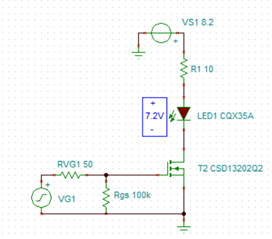
However, rather than a BJT, I would like to control a switch through a function generator that will turn on/off a N-channel MOSFET. I made a porotype of the above circuit with a IRL2703PbF from International Rectifier and it seems to have worked adequately (other than the MOSFET getting fairly warm after 10 ish minutes of operation). I would like to turn my prototype into a PCB using SMD components and was hoping to get some feedback in if I need to consider more than just the SOA, VGS, and power dissipation P = RDS(on)2ID  to pick an appropriate transistor for this application…

Specs of my expected operation conditions:

I will supply the voltage (7.2 V) and current limit (ID = 0.1 A) the LED directly using a separate DC power supply.

The gate of the MOSFET will be directly connected to a function generator (50 Ω output impedance) that will supply 0-5 V square wave with 10 kHz (or 100 µs pulses) modulating frequency with 50% duty cycle. (I.e., VGS = 5 V when ON and 0 V when OFF.)

I am thinking of using the CSD13202Q2. I have done some example computations of parameters below to check for "appropriate" working conditions.

From these specs and using the Fairchild/On Semiconductor FDV305N MOSFET as an example I expect (attached datasheet):

P = (0.1 A)2 * 0.22 Ω = 2.2 mW << 350 mW absolute rating 

VGS(ON) = 5 V >> VGS(th) = 1 V 

VGS(OFF) = 0 V  < VGS(th) = 1 V 

From the SOA figure (below), I expect VDS < 1 V as the LED will drop the 7.2 V applied by the power supply, ID = 0.1 A, and pulse modulation of 100 µs… I am well below the RDS(ON) LIMIT of the plot and in the safe operation range (I think).

Additional considerations:

Since I am directly using a function generator to supply the gate voltage and current, do I need to put a resistor between the gate pin and function generator? If so, is this for power dissipation and/or current limiting purposes?

Do I need to worry about the power dissipation at the gate of the MOSFET? I feel like since this is such a low power operation that I do not need to worry about that.

Do I need to worry about the the bias current needed for the gate (IG)? Based on some technical notes I read, IG = Qgfm = 1.5 nC x 10 kHz = 0.0125 mA (which I expect the function generator to be supplying approximately 50 mA with my operating conditions).

Thank you for taking the time to read my post! I appreciate any insight/feedback in the parameters I need to consider when choosing a MOSFET for pulse based driving of an LED.

FDV305N_D-2312978.pdf

  • Hello Camille,

    I thoroughly enjoyed reading your post and I thank you for your interest in TI FETs. Below you will find a couple links. The first is an app note that includes links to all of TI's web based FET technical information. The second is a recently published app note on avoiding common mistakes with FETs.

    I believe a FET is a better choice than a BJT because it's simpler to drive and there is no need for continuous gate (base) current to keep the FET (BJT) on. The CSD13202Q2 is a good choice and should be easier to work with than some of our smallest FemtoFET devices. Plus it can dissipate ~2W on a multilayer PCB with a good layout. You should be able to drive it with a function generator although the rise and fall times will depend on the current drive capability of the function generator and any external gate resistance. Think of the FET gate as a capacitor that you have to charge to turn on and discharge to turn off. Higher current drive capability results in faster charge/discharge times. The IG calculation is the average current but the peak may be higher.

    When calculating the conduction loss in the FET with a time varying signal (i.e. square wave, sine wave, etc.) you should use Pcond = IDrms² x Rds(on). For a square wave IDrms = ID x √D, where D = duty cycle of the square wave. There will be some switching loss but I think we can ignore it for now. I also have to comment on gate drive voltage. As explained in the common mistakes app note, just because VGS > VGS(th) doesn't mean the FET will be fully on. In order to guarantee on resistance, VGS ≥ min VGS where Rds(on) is specified in the datasheet and tested in production. For the CSD13202Q2 min VGS = 2.5V >> VGS(th). Adding a gate resistor is usually a good idea and it can be 0Ω if not needed. Also, a gate-to-source resistor ensures the FET is off if the gate is left floating. The gate drive power is dissipated in the driver and external gate resistor. Not in the FET. You might also consider a resistor in series with LED to limit the current. If your supply is fixed and you know the voltage drop across the LED you can calculate a resistor value to give you the desired current.

    Safe operating area - you will find a couple of articles in the app note - is mostly a concern when the FET is operating in linear mode in the saturation region where VDS > VGS - VGS(th). There is both voltage across the FET while there is current flowing thru it. In a switching application like yours, the time in the saturation region should be very short during turn on and turn off and SOA is not a big concern.

    https://www.ti.com/lit/an/slvafg3f/slvafg3f.pdf

    https://www.ti.com/lit/an/slpa021/slpa021.pdf

    I hope this helps. Feel free to ask additional questions or let me know if I haven't answered your questions.

    Best Regards,

    John Wallace

    TI FET Applications

  • Hi John,

    I appreciate your insight and feedback on my choice of transistor for the design. I will spend a few minutes digesting what you wrote and follow-up if I have any additional questions.

    At first glance it seems like you touched upon every inquiry I had.

    Thanks

  • Hi John, 

    This is my proper "follow-up" post to your message above. 

    You should be able to drive it with a function generator although the rise and fall times will depend on the current drive capability of the function generator and any external gate resistance.
    Adding a gate resistor is usually a good idea and it can be 0Ω if not needed.
    The gate drive power is dissipated in the driver and external gate resistor. Not in the FET
    The IG calculation is the average current but the peak may be higher.

    Was hoping to elaborate a bit further on these points... having an additional gate resistor seems to be used for voltage/current regulation (i.e., rise/fall time) and power dissipation. The latter makes sense as typically the internal gate resistance (Rig) of the FET is small from what I recall, thus minimal power will dissipate through the gate/FET itself. For the rise and fall time, since my function generator has an output impedance of 50 Ω and I will be supplying 5 Vp square waves, I estimate the rms current supplied by my function generator to be IVGrms = (5 Vp x √D)/50 Ω = 70.7 mA rms, where D = 0.5. I estimated IG for the CSD13202Q2 to be 66 μA for 10 kHz modulation. Sure, I am not currently accounting for peak currents needed for the gate... but since IVGrms is approximately 1000x times greater than IG is that a cause for concern regarding the rise/fall time of the FET?

    I also have to comment on gate drive voltage. As explained in the common mistakes app note, just because VGS > VGS(th) doesn't mean the FET will be fully on. In order to guarantee on resistance, VGS ≥ min VGS where Rds(on) is specified in the datasheet and tested in production. For the CSD13202Q2 min VGS = 2.5V >> VGS(th).

    Thanks for elaborating on this. Read the app note and will ensure that my driver is a N-Channel FET low side switch configuration and that VGS = 5.0 > 2.5 V min VGS where Rds(on) = 7.5 mΩ which should suffice to turn on the FET. 

    Adding a gate resistor is usually a good idea and it can be 0Ω if not needed. Also, a gate-to-source resistor ensures the FET is off if the gate is left floating.

    Referred to the 2nd link for this as well. It mentions anywhere between 10k-1MΩ for RGS seems to suffice. Does this resistor also act as a power dissipater? Does it serve any other purpose other than ensuring to prevent floating gate and corresponding complications to the FET? I currently just picked a value of 100 kΩ for my circuit design below.

    With your advice/clarifications and app notes (mainly the second link) I went about and made a draft of my LED driver using the CSD13202Q2 shown below:

    The LED I am using is rated to typically have a 7.2V forward voltage at 0.1 A forward current at which I use R1 = 10 Ω and VS1 = 8.2 V to limit the current to 0.1 A. (Ignore the LED model, it is used for illustrative purposes here only and does not represent the actual LED I will be using.)  RGV1 represents the 50 Ω output impedance of the function generator (VG1). 

    I expect the rms conduction loss of this driver to be roughly 37.5 μW, which is well below the rated 2 W limit. If I were to reconfigure the supply voltage value such that the IDrms becomes 0.1 Arms (i.e., 0.141 A peak), the power dissipated by the FET will be 75 μW.

    There will be some switching loss but I think we can ignore it for now

    I agree, seems like switching loss is more of an issue for more sophisticated switches like buck converters (the excel sheet tool you made to check FET combinations for switching loss is really well done), and I presume I do not need to worry about it for this small of a application. 

    Thanks again for your insightful comments and taking the time to read and share your knowledge. This has helped me greatly!

    Cheers

  • HI Camille,

    I am off for the Thanksgiving holiday this week and will get back to you when I return next Monday.

    Thanks,

    John

  • Thanks for letting me know, John.

    Have a great holiday break!

    Best,

    Cam

  • Hi Camille,

    An external gate resistor is used to control the rise and fall time of the FET switching. Most commonly used in switch mode (i.e. DC-DC, motor drive, etc.) where the FET is switching at kHz or MHz. If not required, it can be populated with 0 ohms. The gate-to-source resistor is mainly to avoid unintentional turn-on if the gate is left floating. It should only dissipate a minimal amount of power. A 100kΩ resistor is a good starting point and it can be adjusted.Your schematic and drive scheme looks good. Let me know what else I can do to help.

    Thanks,

    John

  • Hi John,

    Hope you had a great thanksgiving. I appreciate additional input on my design!

    Happy to say I will be moving on to design a prototype board with Altium.

    Best,

    Cam

  • Hi Camille,

    Great, let me know if I can be of further assistance.

    Thanks,

    John