This thread has been locked.

If you have a related question, please click the "Ask a related question" button in the top right corner. The newly created question will be automatically linked to this question.

UCC28C42: Application Design Consulting

Part Number: UCC28C42


Tool/software:

Dear Experts,

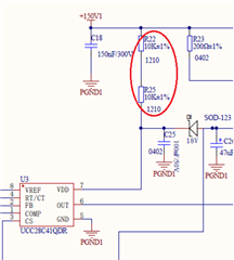
We are designing a BUCK circuit with a wide input voltage using UCC28C42. The input voltage is DC 20-300V and the output voltage is 12V 3A. We want to use the primary auxiliary winding as feedback. The schematic diagram we designed is as follows. During testing, the chip was damaged. We would like to know how to implement this primary feedback and provide some design suggestions. Thank you

  • Hi,

    Your circuit shows VDD connected to 150V through R22 and R25 which total resistance is 20k. VDD abs max = 20V, so the current into VDD in normal operation is about 3mA, So when Vin > 80V, VDD > 20V, then > abs max VDD, so this is likely the reason to damage the IC.

    A typical design is to increase R22 and R25 to only provide a startup current 0.1mA at minimum input voltage, but your input voltage is with a wide range with minimum 20V, so in your case, it looks you need to add an external Zener diode between VDD and GND to clamp the voltage between 16V and 20V so to limit VDD below its abs max. You can try this to see if the issue can be resolved.