This thread has been locked.

If you have a related question, please click the "Ask a related question" button in the top right corner. The newly created question will be automatically linked to this question.

LM5143: LM5143's output current capability has turn worse

Part Number: LM5143

Tool/software:

Hello TI experts,

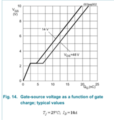
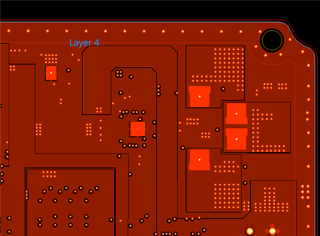
The project we designed  used the LM5143+4pcs MOSFET dual phase architecture. input=16-32V ,output voltage= 14.4V, the current max 20A. The output current can reached 12A. Schematic as attached. There is no problem we mass-produced last year.

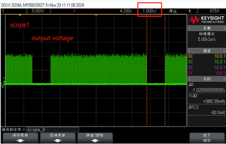
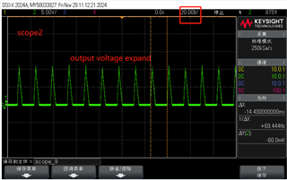
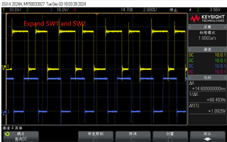
However, we recently mass-produced a batch and found that its output current capability has deteriorated,The component used is from the same batch left over from last year,the output current reached 5A the voltage not stability. please refer to the scope1 and scope2.  The result seems the loop unstable.

I have verified the following steps.

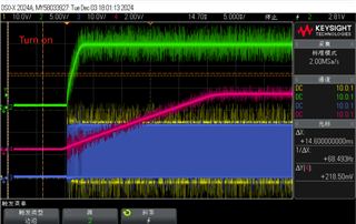
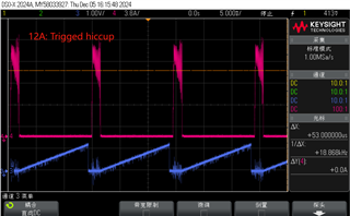
1.the Currently mass production:output current=6A begin unstable.  please refer to scope3. 

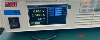
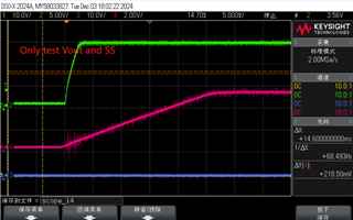
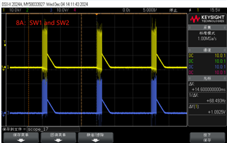
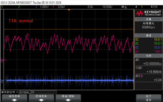
2.Change the 4pcs mosfet form the PCBA mass production last year, the output =9A begin unstable.  please refer to scope4. 

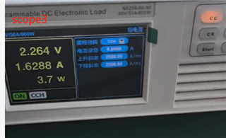
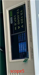
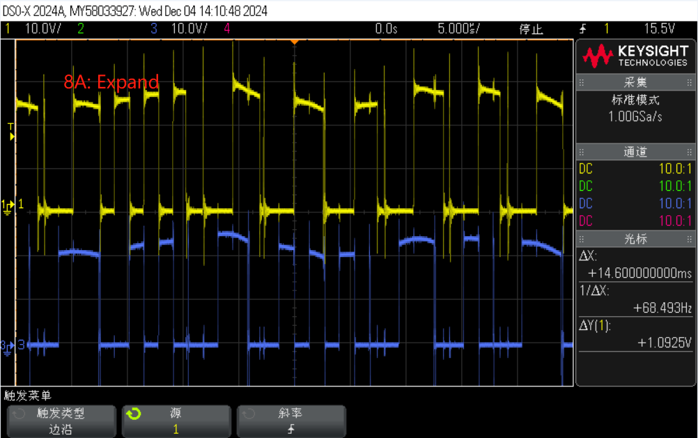
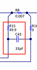
3.Populated the R65031,R65030 and C65051,C65050 can reached 12A no problem,Please refer to scope5.  however the these 4pcs resistor and caps is also depop in production last year.

Please help analyze what difference is causing the abnormal performance of this batch of PCBAs. Looking forward to your reply.

Thank you.

BR Victor


5047.LM5143.pdf

  • Hello Victor

    Can you please fill the design calculator and share it over the thread?

    Here is the link for it - LM5143DESIGN-CALC Calculation tool | TI.com

    Thank you

    Regards

    Onkar

  • 0211.LM(2)5143-Q1 quickstart design tool - revB2.xlsm

    Hello Onkar,

    Please confirm the attached file, Thank you.

    BR Victor

  • Hi Victor

    I reviewed your schematics and the compensation components look fine to me. However, I noticed that the input filterlacks damping, which could potentially leads to instability. I would recommend you go through AN-2162 Simple Success With Conducted EMI From DC-DC Converters (Rev. C) for guidance on designing a damping network. That said, I am not sure if this is the root cause of issue you are observing.

    To better understand the problem, could you please share the SW node, Vout and SS pin waveform during startup.

    Thank you

    Regards 

    Onkar

  • Victor,

    The problem is you're using standard-level MOSFETs not suitable for use with the 5V gate drive of the LM5143. You can see in the plot below the Miller plateau voltage is too high, so there is hardly any gate voltage overdrive.

    Instead, use logic-level MOSFETs with Rdson rated at Vgs = 4.5V (the Miller plateau should be ~3V then). If Vin-max is 32V, then 40V MOSFETs should be fine (see the EVM components for example).

    --

    Tim

  • Hi Onkar 

    I clicked the wrong button, and this issue has not been resolved yet.

    The tested socpe for your reference. (Green: Vout, Pink:SS , Yellow:SW2, Blue: SW1)


    Please confirm them. 

    I am confuse that the same circuit and software why the currently productions have problems, I suspect it may be contamination in the storage of electronic component.

    Thank you.

    BR Victor

  • Hello Tim

    Thank you for your feedback.

    The MOSFETs that has beenopulated on the PCBA is BUK9Y25-60E. I changed the BOMList from BUK7Y4R8-60E to BUK9Y25-60E a long time ago, but I forgot to change the schematic The characteristic is the logic level MOSFETs you mentioned, and the parameters si as shown.

    I am confused that the same circuit and software why the currently productions have problems,  Last year's product was fine. I suspect it may be contamination in the storage of electronic component.

    Thank you.

    BR Victor

  • Hello victor

    Thanks for sharing the waveforms. Are these waveforms taken at 12A load current? SW2 waveform looks okay however, SW1 is alternating between wide and narrow pulses. Could you probe inductor current of phase 1 to see if there any subharmonic oscitations present in the circuit?

    Regards 

    Onkar

  • Hi Onkar 

    The waveforms taken at 3A(light load). 

    8A Load current has issue please refer the scope as below:


    Tomorrow I will probe inductor current of phase 1 and phase 2.

    Thnak you.

    BR Victor

  • Hello Victor

    From the waveforms it looks like hiccup mode is triggered. with Cres = 220nF, t_res (hiccup delay) is around 13 ms. Non switching time in your waveforms looks pretty close to this number. Could you please probe Cres voltage along with inductor current to confirm the issue?

    Thank you

    Regards

    Onkar

  • Hello Onkar

    It triggered hiccup mode.Please refer the scope.(Pink :Current, Blue: Vres)

    I found that although there is no problem with the 11A load, there is significant signal jitter on the Vres.


    Thank you.

    BR Victor

  • Hello Victor

    From inductor current waveforms, loop looks unstable. Could you please try testing same with following compensation values?

    Rc1 221 kOhm
    Cc1 150 pF
    Cc2 15 pF

    Moreover, could you please try using rc filter across current sense resistor as shown in LM5143-Q1 EVM User's Guide (Rev. B)?

    Q: there is significant signal jitter on the Vres.

    I think that's your probe picking the noise.

    Thank you 

    Regards

    Onkar Bhakare

  • Hello Onkar,

    I tried the parameters you suggestions RC1=220K(no 221k resistor on hand) Cc1=150pF, Cc2=15pF.

    It cannot operated normally when unloaded. Please see scope for SW1 and SW2.


    I have two questions to confirm with you:
    1. If the loop is unstable, why is the waveform of SW1 normal and only SW2 is alternating between wide and narrow pulses.

    2. you Mentioned the rc filter across current sense resistor is for example as below?


    Thank you.

    BR Victor

  • Victor,

    Can you update the quickstart for the correct ESR of the electrolytic output caps - two caps at 60mΩ each will be 30mΩ net (the ceramics in parallel won't make much difference). Try crossing the loop over at 20kHz to get it stable, then test the load transient response and adjust the crossover higher as needed.

    Also, the current limit at 33A seems high here if 6-20A is the Iout spec - consider increasing the shunt resistors to 5mΩ and the inductors to 6.8uH to optimize the power stage.

    I see you have a high value for upper FB resistor, 230k, which may be susceptible to noise. Trying dropping the FB resistor to get slightly above 5kΩ parallel combination. Finally, no need for the 2.2uF directly on the VOUT2 pin.

    Regards,

    Tim

  • Hello Tim,

    I updatad the quickstart  excel,  The current parameters look fine.

    I approve with your suggestions to optimize power,  have also tried modifying the FB resistor and removing the VOUT2 capacitor, but the current issue has not been resolved.

    Currently, Populate the R65031, R65030 and C65051, C65050 are effective. I would like to confirm the cause of this issue and any risks for these?

    Thank you.

    BR Victor

    6177.LM(2)5143-Q1 quickstart design tool - revB2.xlsm

  • Victor,

    Just looking at the waveforms again, you may be hitting current limit at startup (1640uF is a huge Cout at 16V output) and triggering hiccup. Check the startup waveform for Vout.

    Try increasing the SS cap or decreasing Cout. Or use the RES pin to disable hiccup.

    Regards,

    Tim

  • Hi Tim,

    My problem is not limited to startup.

    Slowly increasing the load current to a level of 12A after startup can also cause this issue,
    Of course, this problem can occur even when powering on at this load level, and even when powering on at 11A.

    I tried to increase Css from 100nF to 220nf, but the result was still the same,I don't have a suitable output capacitor on hand and haven't tried it.

    I will be on a business for a week. I apologize for the delayed response to the message.

    Thank you.

    BR Victor

  • Victor,

    Try adding Ceramic Cout. Send on your layout for review.

    Regards,

    Tim

  • Hello Tim,

    Please review the layout:   


    ​Thank you.

    BR Victor

  • Hi Victor,

    The switch node copper areas are quite large here and includes vias to internal layers (which disrupt the internal GND plane). In general, we recommend to minimize the SW copper area as it is a radiating plane with high dv/dt - there shouldn't be any internal SW copper area either. See app note SNVA803 for more detail. There should be a quiet GND island for AGND, especially as the controller is very close to the power stage in this design. Refer specifically to the EVM layout and the layout guidelines in the data sheet.

    Please check that the VCC caps are right beside the VCC and PGND pins. Also the boot caps should be close to the BOOT and SW pins. The EVM layout template is what should be replicated here.

    Regards,

    Tim

  • Hi Tim,

    Thank you for reviewing the layout.


    I am still curious that this design was frozen last year. The PCBA produced last year had no issues but this batch has issues this year.

    I just learned that this PCB is newly produced this year, and the schematic and layout design were frozen last year. There have been no changes since then I am also currently confirming the PCB process and stacking configuration.

    Do you have any suggestions here? Thank you again for your assistance.

    ​Thank you.

    BR Victor

  • Victor,

    Maybe you can review what changes were implemented on the new PCB.

    Regards,

    Tim

  • Hi Tim,

    Thank you, I already have done it.

    BR Victor

  • Hi Victor, were you able to resolve the issues?

  • Hi Tim,

    Sure ,thank you for your support.

  • Thanks, Victor. I'll close out this thread.