This thread has been locked.

If you have a related question, please click the "Ask a related question" button in the top right corner. The newly created question will be automatically linked to this question.

UCC28070 used for single phase

Other Parts Discussed in Thread: UCC28070

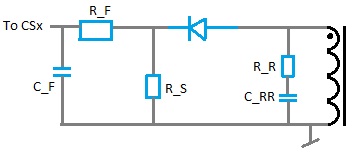
I am working on a scalable PFC boost design that will use only one phase of the UCC28070 for a lower output power variant. The full power model uses both phases interleaved and the lower power model depopulates one of the phases.

  • Is there anything special I have to do to disable one phase? 
    • I have the disused current sense input grounded
  • Does it matter which of the phases I use in single phase mode? 
    • I am currently using phase B for single phase.

Thank you!

  • The UCC28070 interleaved PFC can be used for single phase and it shouldn't matter if you use phase A or B.

    I would do a few things to the IC to make sure that noise does not couple into the IC.

    1. Populate the current amplifier that is not being used.
    2. You may want to have a resistor on the CS pin that is not being used as well.

    It is always a good idea not to have open pins on a PWM IC in a power supply to avoid possible noise related issues.

  •  

     We used UCC28070 running 2 phase for full load and disable one phase when load decrease to 50% of full load, Can we disable either A or B automoticly when output power decrease about 50% of full load?

  • You can properly do it by connecting external comperators to the FB/control network and thereby disable it.

    You should properly measure the output current (e.g. using HV7802) and then make sure you use a hysteresis for when you use one or two phases.

  • As suggested by “CWilson”, an external comparator can be used to detect the load level and disable or enable either of the phases.

    An alternative to detecting load current is to monitor the VAO voltage, which is a good indication of output load power. Read this with the attached files as references.

    Since the UCC28070 incorporates input voltage feed-forward, the voltage-loop error-amp output (VAO) is largely independent of line variations, except for some minor error due to the quantization of the feed-forward.

    The comparator output is suitably connected to the gate-drive circuit of the phase to be disabled at light loads.  This is the minimum required to accomplish phase management.

    In addition to simply disabling the gate drive, two additional modifications can be implemented to improve performance:

    1. Double the resistance on the IMO pin, to avoid disturbing the PFC output voltage and input current, and
    2. Ground out the CAO output of the phase being disabled, to avoid a current spike when that phase is re-enabled.

    See the attached file on Phase-Management Demo to compare the performance differences.

    Also see the controller and power-board schematics (SLUR032 and SLUR033) to assess a sample implementation on a 1200W evaluation design.  Note that this design incorporates phase-management using a manual switch rather than an automatic comparator circuit.  (There are a number of other switches, jumpers, and additional components in this design intended for evaluating performance under various operating options, and are not normally needed in a “real-world” design.)

    Sufficient hysteresis is useful to avoid jumping between 1-phase and 2-phase operation during minor load and line perturbations.  The amount of hysteresis depends on the typical degree of line/load variation around the phase-drop threshold. 

    Testing has shown (see file on efficiency gain) that efficiency improvement becomes significant mainly below 30% of load, so setting the phase-drop threshold close to 50% load may be too restrictive to the amount of hysteresis available.   A threshold at 30% or lower allows a wide hysteresis to avoid “chatter” on minor line/load variations. 

    Finally, do not load the VAO output with resistance; it should only see the impedance of the compensation network and nothing more.  Any hysteresis network should be in the reference input of the comparator.  Appropriate circuitry is then added to the output of the comparator to disable the gate-drive, ground-out the CAO, and double the IMO resistance.

    Regards,

    John

    UCC28070-7-24-12 (2).zip
  • Hi John,

    Do you have a desciption of when the phase management starts?

    I have 2x UCC28070 IC's which behaves differently, so it would be nice to know when and why the phase B is enabled and disabled.

    /CWilson.

  • Hi,

    There is no designed in phase management system on the UCC28070.

    John

  • Hi John,

    Do you have a BOM of the 1200W demoboard? I need info regarding the D5, D6 and D7 (on slur032.pdf) since I need to clamp my CS-voltage.

    Kind regards,

    CWilson.

  • I think the BOM is wrong..??

    According to slur030.pdf (http://www.ti.com/lit/ml/slur030/slur030.pdf) the zener i 33V?.. The input is limited to 3.6V accroding to the datasheet?.. Is it a 3V3 zener instead?

    I have:

    1:100 turns, R_R = 330R, C_RR = 22p, D = 200V/1A, R_S = 10R, R_F = 1k, C_F = 220pF. => This should give me approx. 2V at max current, which I also seems to measure - but I'd like to attenuate/clamp the ringing at turn-off - it's above 4-5V and I think it kills the CSA and CSB inputs.

  • I believe you misunderstands the purpose of the 33V zeners.


    First, the BOM is NOT wrong.

    The 33V zeners are used to clamp the reset voltage on the CTs, not to clamp the signal itself.


    Second, 4-5V ringing on CSA and CSB cannot kill those inputs; they have a +7V Abs Max rating.

    But they should not have any input voltage go below GND.


    However, significant ringing after turn-off may be indicative of a different problem.

    Since you says  “D = 200V/1A”, this suggests you are using a power diode to rectify the CT output.

    This kind of diode is too big, and has too much reverse recovery and junction capacitance.

    You should be using a signal diode (typically 4ns trr and ~4pF) as listed in the BOM.


    You have got some parts whose purpose I can’t identify: R_R and C_RR are mysteries to me.

    R_S is the sense resistor at 10R, and I believe R_F and C_F form an R-C filter to the CSx inputs.

    These sound okay, provided the 220ns time constant does not significantly degrade the CSx waveform.  

    What are the R_R and C_RR  for… Do you really need them?


    Third, I think you should use a higher value R_S.  A 2-V peak at maximum current is underutilizing the capability of the multiplier range.

    It is good for 3.6V and I recommend that you use all of it.  This suggests a value of 18R.  

    (Changing this may require changing some other resistor values as well, to match the scaling.)

    If the CSx signal exceeds 3.6V, it will not clip internally, but kind of has a soft non-linear compression above 3.6V.

    You get a little distortion, but not much even up to 4V input and then it starts to flatten out more rapidly.

    Regards,

    John

  • The IC went dead (duty cycle to max) when I turned the voltage down from 260VAC towards 230VAC. Suddenly strange noise and duty at 97%.

    Q: Should I limit the duty cycle to e.g. 75% (70% is theoritical limit when boosting from 85VAC to 400VDC) - can this be done on the DMAX resistor? It's not done in the app-note (http://www.ti.com/lit/an/slua479b/slua479b.pdf) which I calculated my resistors/caps/inductors after. Please see equation 37 page 10.

    The converter worked fine before. I run full load from 160V to 260V (which is the purpose) and had no problems going from 85V-160V (de-rated output power) and then 160V-260V (full power).

    R_R and C_RR is the resistor and capacitor of my reset network of the current transformer. They are in series and are coupled from "+" on current sense trafo to "-".

    I'll try to change the diode to a 1N4148 200mA 75V 4ns and see if that dampens the ringing.
    The currently diode is 15ns STTH1R02 (Farnell 1295245).

  • Please send the two current sense signals and  the current sense amplifier outputs at 260 V and 230 V input voltage.

    Repeat with the voltage amplifier output with the current sense signal.

    Use a time base that lets us see the current sense signal.

    John