TL431: Inquiry Regarding Specification Change for TL431 PCN

Part Number: TL431

Tool/software:

Hi Support Team,

We have some clarifications to seek regarding the recent PCN (Product Change Notification) for the TL431. Specifically, we would like to confirm the following points:

  1. Impact of Connecting Pin 2 to CATHODE/REF:

    • Many of our applications involve connecting Pin 2 to both the CATHODE and REF terminals. Could you clarify what specific issues or problems may arise from this configuration under the new specifications? Are there any scenarios where this connection method could result in device malfunction or performance degradation?

  2. Scope of the Change:

    • The PCN indicates a change in specifications. Can you confirm whether this involves only a change in the documentation or if there are internal modifications to the product itself? Specifically, does the new specification arise from an internal design change that might introduce issues when Pin 2 is connected to both CATHODE and REF, necessitating a change in usage guidelines?

We would greatly appreciate your prompt response as this will help us assess the necessary steps for compliance and application adjustments.

Thank you for your suppor

Thanks,

Conor

  • Hello Conor,

    Can you please provide the full part number for TL431 that is being used? Since there are multiple package options for TL431, I want to make sure I provide up to date information for the correct package.

    Thanks,

    Jackson

  • Hi Jackson,

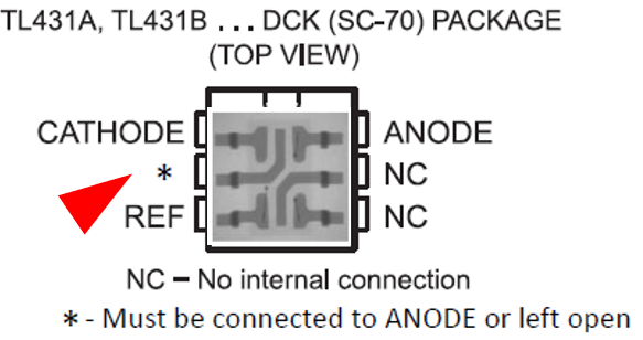
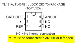
    I am writing to seek clarification regarding PCN Notification# 20240614001.0, specifically concerning the DCK package devices (e.g., TL431AIDCKR and TL431BIDCKR). Based on the PCN, datasheet updates, and my technical analysis, I would like to confirm the following points

    Q1. Based on X-ray inspection results, it appears that the lead frame of Pin 2 in the DCK package is connected to the backside of the chip. Is this interpretation correct?

    Additionally, I noticed that Pin 5 seems to have a similar internal lead frame structure. However, the updated datasheet does not impose the same connection restriction on Pin 5. I assume this is because Pin 5 has a different internal function or its impact on device behavior is negligible compared to Pin 2. Could you please elaborate on this point?

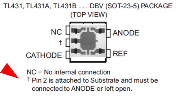
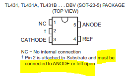
    Q2. In the DBV package, it is clearly stated that Pin 2 is connected to the substrate and must either be tied to the anode or left open. Does the same restriction apply to the DCK package?

    Q3.
    Given the proximity of Pin 2 to the chip backside, I assume that it is susceptible to capacitive coupling. If Pin 2 is connected to the cathode or REF pin and a steep voltage change (dv/dt) is applied, it seems plausible that parasitic capacitance could impact the cathode voltage. Is my understanding correct that the primary factor influencing this behavior would be the dv/dt of the voltage change applied to Pin 2? If this is correct, understanding the degree of impact would be critical in evaluating replacements for the device.

    Q4.
    "There are no changes to the actual device" on PCN means that there have been no physical or electrical changes to the device itself. The origin of this change suggests that there have been no changes to the device since its launch. However, the changes to the datasheet (especially the clarification of the pin connection constraints for the DCK package) are due to this PCN.
    Is my understanding above correct?

    Thanks,

    Conor

  • Hi Conor,

    Based on X-ray inspection results, it appears that the lead frame of Pin 2 in the DCK package is connected to the backside of the chip. Is this interpretation correct?

    Pin 2 previously had no internal connection, but after the PCN update it is has some other connection.

    Additionally, I noticed that Pin 5 seems to have a similar internal lead frame structure. However, the updated datasheet does not impose the same connection restriction on Pin 5. I assume this is because Pin 5 has a different internal function or its impact on device behavior is negligible compared to Pin 2. Could you please elaborate on this point?

    This understanding is correct. Pin 5 has no internal connection (NC) while Pin 2 has some other connection.

    In the DBV package, it is clearly stated that Pin 2 is connected to the substrate and must either be tied to the anode or left open. Does the same restriction apply to the DCK package?

    Pin 2 of the DCK package must similarly be connected to the anode or left floating, but it does not necessarily have the same exact internal die connection.

    Given the proximity of Pin 2 to the chip backside, I assume that it is susceptible to capacitive coupling. If Pin 2 is connected to the cathode or REF pin and a steep voltage change (dv/dt) is applied, it seems plausible that parasitic capacitance could impact the cathode voltage. Is my understanding correct that the primary factor influencing this behavior would be the dv/dt of the voltage change applied to Pin 2?

    It is accurate that there could be effects on the cathode voltage or other device operation if pin 2 connections do not follow the updated datasheet recommendations. The datasheet does not provide information on how voltages, ramp rates, or other connections for pin 2 other than the official recommendation affect device operation.

    "There are no changes to the actual device" on PCN means that there have been no physical or electrical changes to the device itself. The origin of this change suggests that there have been no changes to the device since its launch. However, the changes to the datasheet (especially the clarification of the pin connection constraints for the DCK package) are due to this PCN.
    Is my understanding above correct?

    The PCN is to outline that there are no changes to the device performance as defined by the datasheet, except those specifically outlined in the PCN.

    In general, I would strongly recommend making sure that pin 2 of the DCK package is left floating or connected to the anode as the datasheet suggests.

    Please let me know if there are any further questions.

    Thanks,

    Jackson