LM25085: Unstable regulation behavior

Part Number: LM25085

Tool/software:

Hi

I designed a Step Dawn power supply based on the typical application of the LM25085 .

In my application noise is not an issue, nor current limiting, so is the simplest possible design.

That said it required to sustain the output voltage from no load to 3A load, while load is applied at once, it fails.

When current rises from 0 to 3A the output voltage falls from 12V to 2 for 200mS then rises to 7V for 900mS and after that it rises again to the 12V. That is not acceptable.

I played with capacitors values, but wasn't able to make it work.

Please advice.

Eli Jacob 
eli@global-rd.com

  • Hello Eli,

    What kind of load are you using? 

    What are the conditions of this load transient test?

    Best regards,

    Ridge

  • Perfect Resistive load

  • Hi,
    I continued "playing" (knowing PS control loops): 
    I completely removed C102 (15nF)
    I changed R107 to 3.3K in order to be sure CL in never reached
    Still didn't work correctly.
    Added a 220pF capacitor by hand on C102, no effect. Taken off the capacitor START WORKING
    And here is the interesting part:
    it kept working, I could turn ON and OFF the load getting a drop of 0.5V and 1V ripple, is a bad regulator but enough for this simple case. The board doesn't heat up over a few degrees with this load.
    I let it powered without load for 15min to completely cool down and then again it doesn't work. It is needed to touch again with any capacitor in c102 and let go to start working, and then it will keep working till it cools down.
    Any idea how to fix this device? 

  • Hi Eli,

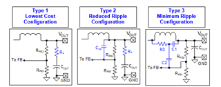
    I reviewed your schematic, and notice that you do not appear to have an output ripple configuration shown. 

    This device uses a constant on time (COT) control architecture, which means that a certain amount of ripple is required on the FB pin of the converter so that it can operate properly.

    It looks like the start of Type-2 injection is used with the feed-forward capacitor (C102), but a resistor in series, or sufficient ESR, with the output capacitance is required for the ripple injection to function properly. It may be that this unstable behavior is due to insufficient ripple on the FB pin of the device.

    Here are the different types of ripple injection:

    The best performance will be with Type-3, and it will allow you to have very low output ripple since the injection network will generate the ripple you need from the inductor current. 

    Since it looks like you are already using something close to Type-2, you could try adding the resistor in series with Vout. 

    The device calculator can help you determine this value: https://www.ti.com/tool/LM25085-5085QUICK-CALC

    Make sure to click "enable content" at the top of the worksheet so that the calculations function with your inputs.

    Are you able to share your layout for review? Layout is also critical to proper operation of a buck controller.

    Best regards,

    Ridge

  • I will try to add a series resistor and post the result

  • Hi

    The current series resistor generated by the layout was about 10mohm I tried adding till 0.22ohm.
    With 0.22ohm after loading the voltage drops to ~4V and stays there never coming back to 12V.

    BTW the calculator doesn't run correctly on my PC, I get errors:

  • Hi Eli,

    Are you able to share waveforms of the FB, SW, and Vout nodes?

    Can you also provide the PCB layout?

    With regard to the calculator, I'm not sure what the issue would be. It is an excel worksheet, and must be opened with excel. It may be that the Libre software you are using is incompatible with the document.

    Best regards,

    Ridge

  • Hi
    Sorry that I am not allowed to share the PCB layout, however all the lines are short.
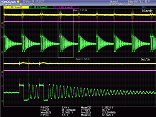
    Here are the signals with minimal load:

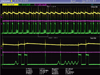
    Here are the signals with 4.4ohm load:

    Magenta is Vout 12.2V without load, 3.24V with 4ohm load
    Yellow is FB 1.27V without load 3.5V with 4ohm load, you can see the big ripple
    Green is SW

    That waveforms are with the 0.22ohm series resistor to the 66uF capacitors

    Thanks for your fast answers

  • Hi Eli,

    I will continue to review this issue and reply by early next week.

    Best regards,

    Ridge

  • Hello Eli,

    Are you able to share the PCB layout?

    Best regards,

    Ridge

  • Hi 
    I am not allowed to share the layout but I can describe: The GND and Vin are planes, the MOSFET drain diode cathode and Inductor are a small plane, other signals are very short traces.
    If on the contrary some signal require uncommonly longer traces please comment.

  • Hi Eli,

    Layout is very important for controllers, and there may be something in the layout we can change which helps this issue.

    I think it is an important step for us to review the layout to best help solve this problem.

    Are you able to share the layout via private message with TI? I understand that you may not want to post the files on a public forum.

    Best regards

    Ridge

  • Hi
    I want to thank you for your effort helping me to solve this issue, however I must inform you that I finally solve it by replacing the device with an other from your competition on the far east (after a small PCB layout change) 
    I always prefer to select my components from our friends (in USA and specially TI) but I got to the conclusion that even if I make it work it will be boundary stable, therefore I replaced the device with a functionally compatible one, that worked effortless.
    I would recommend a revision on the silicon and perhaps making a pin compatible always working option.
    Thank you again
    Eli Jacob
    Global R&D ltd