Tool/software:
Hi,
I designed a boost converter with LM5177, input voltage is 9V to 60V, the output voltage should be 57V.
When I give power the board didn't work. I shared the schematic of my design, Can you check it and help me to fix it?
This thread has been locked.
If you have a related question, please click the "Ask a related question" button in the top right corner. The newly created question will be automatically linked to this question.
Tool/software:
Hi,
I designed a boost converter with LM5177, input voltage is 9V to 60V, the output voltage should be 57V.
When I give power the board didn't work. I shared the schematic of my design, Can you check it and help me to fix it?
Hi Kerim,
can you check the voltage level the VCC pin.
You are working with quite high voltage levels on input and output but within your schematic I do not see any gate resistors or snubber. So you might have large under or overshoot on the SW node (SWx) which can violate the abs max ratings and lead to a damage of the device.
Best regards,
Stefan
Hi Stefan,
thank you for your answer, I checked the VCC it is 5V. Should I add gate resistor or snubber? Which one will be the best choice? I have checked the evoluation board there is 3 ohm resistor and 10nf capacitor. Do you mean like this resitor and capacitor? Will 3ohm and 10nf be enough?
Best Regards,
Kerim
HI Kerim,
if VCC is 5V then this OK.
So lets keep the gate resistor and snubber in the backlog for an design update. Also add filter for CSA/CSB here
The issue needs to be somewhere else, so please check:
Probe:
- EN/UVLO, SS, VIN, VOUT
- SW1 and SW2
Disable the current limit to reduce the options for issues:
- put IMONOUT to VCC
Best regards,
Stefan
Hi Stefan,
I want to be sure, Do you mean I need to connect IMONOUT directly to VCC , with no resistor or RC filter required? Then I will measure the pins you want me to check.
Best Regards,
Kerim
Hi Kerim,
yes, this will just disable the average current limit.
Best regards,
Stefan
Hi Stefan,
I connected IMONUT directly to VCC, then I measured these pins and the results were;
EN/UVLO = 1.5V
SS = 0,47V
VIN = 11,40V
VOUT = 46V
SW1 = 0,165V
SW2 = 0,165V
Best Regards,
Kerim
Hi Kerim,
sorry for not being clear enough.
Can you probe them with a scope?
From above it looks like the device is continuously restarting.
You can also try to increase the SS cap to e.g. 100nF.
Best regards,
Stefan
Hi Stefan,
Sorry for the late reply, I wasn't at the office.
I shared pictures, the names of pictures are same as the name of tests. I tested them with 100nF SS cap.
Best Regards
Kerim
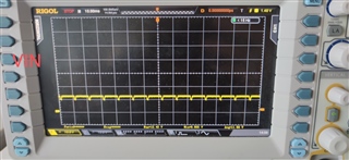
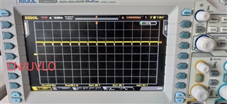
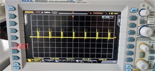
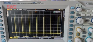
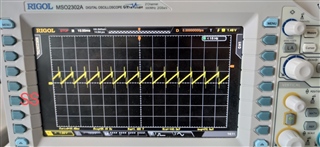
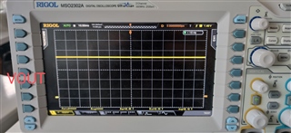
Hi Stefan,
as you can see from the SS plot the device is continuously restarting shortly before reaching the 1V.,
Can you try to increase the SS cap to e.g. 150nF as a first step.
The probe VIN, SW1 and SS in one plot.
Best regards,
Stefan
Hi Stefan,
my scope has 2 probe, sorry for that. I shared the measurment result, with 150nF SS cap.
Best Regards,
Kerim


Hi Kerim,
sorry for the delay, accidentally i set the wrong tracking flag for the thread.
Checking the scope plot showing VIN, it looks like the supply drops the moment the controller starts to operate and the VIN voltage drops below the UVLO level set with the resistor divider on EN/UVLO.
Check if the supply could be more stable and does not drop. Check current limit, add buffer caps,...
Try to set the UVLO trigger to a lower voltage level.
Best regards,
Stefan
Hello Stefan,
No problem, thank you for your help.
I obtained the value shown in the images when no load was connected, and I was able to achieve the desired voltage level in the absence of a load.
However, when I connect a load, the output voltage drops, and depending on the load, it can decrease by as much as 3 volts.
Best Regards,
Kerim


Hi Kerim,
so without load you get the required output voltage and this also looks stable?
If you add load the output voltage drops - right?
How does the load correlate to the load. Is this linear? Does it drop even with very small load? .....
From the schematic it does look like that you do not have the filter at CSA/CSB can you try to add that?
Would be also good to see the layout - esp. the connection of CSA/CSB to the controller (once above questions are clarified)
Best regards,
Stefan
Hi Stefan,
Thank you for your response.
Yes without load voltage looks stable.
Yes, when I add load to the output voltage drops
It is a smart load. Yes it is linear. Yes I just arrange the load to pull 40mA again the output voltage droped
Maybe it will be difficult to add filter at CSA/CSB. I think maybe my problem is deal with the layout. it looks bad.
Best Regards,
Kerim.


Hi Kerim,
yes, i also think the layout needs to improvement and that the issue most properly is due to noise pickup into CSA/CSB lines.
This are very sensitive and most responsible input for the control loop. Therefore there are dedicated pins to have them as Kelvin connection to the Sense Resistor available. Also a filter should be added esp. with higher voltage or power levels.
For layout guidelines the layout please have a look at this application report first: https://www.ti.com/lit/pdf/slvafj3
Additional info on layout (based on another device but also valid in most cases for the devcie) can be found here :
(1) Four-switch buck-boost layout tip No. 1: identifying the critical parts for layout
(2) Four-switch buck-boost layout tip No. 2: optimizing hot loops in the power stage
(3) Four-switch buck-boost layout tip No. 3: separating differential sense lines from power planes
(4) Four-switch buck-boost layout tip No. 4: routing gate-drive and return paths
Best regards,
Stefan
Hi Stefan,
Thank you so much for your help.
I will redesign my board based on the guidelines you shared. Prototyping will take time.
When I get the new board, I will test it and then inform you.
Best regards,
Kerim
Hi Stefan,
I hope this message finds you well.
I have started a new design for my project that we discussed earlier. I used the LM5177 Quick Calculator, and I have attached the document. Could you please take a look?
If there are any issues, please let me know.
Best regards,
Kerim
Hello kerim,
Due to year-end vacation, answer are delayed and not as detailed as typically.
As long as none of the fields in the calculator is red, everything should be OK.
Please start your design with these values and follow the layout recommendations in the datasheet and application note.
Best regards, Brigitte
Hi all,
I have finished my design, Could you check it please ?
In my project;
VIN= 9V~60V Vnominal= 24V
Vout= 57V
Mosfets are BSC034N10LS5ATMA1.
I used LM5177 Quick Calculator. you can see it at the upper.
Best Regards,
Kerim
Hi kerim,
We will look into this and come back to you.
Best Regards,
Feng
Hi Kerim,
Please see below my review list and bold marked line items which should be checked again (Note: other info are left here to give an overview of what has been checked)
Schematic:
For layout guidelines the layout please have a look at this application report first: https://www.ti.com/lit/pdf/slvafj3
Additional info on layout (based on another device but also valid in most cases for the device) can be found here :
(1) Four-switch buck-boost layout tip No. 1: identifying the critical parts for layout
(2) Four-switch buck-boost layout tip No. 2: optimizing hot loops in the power stage
(3) Four-switch buck-boost layout tip No. 3: separating differential sense lines from power planes
(4) Four-switch buck-boost layout tip No. 4: routing gate-drive and return paths
Best regards,
Stefan
Hi Stefan,
Thank you for your response,
I have added filter Cap. to Risns and snubber to SW1. I shared it please check. If it is okay, I will start to design with you layout recommendations.
Best Regards
Kerim.