


Tool/software:
Hi,
Does there have any caculator tool for TPS61287 compensation can share to us?
Or have any suggest value for Vin 20V to Vout 24V/3A?
Please help review below schematic for Vin 20V to Vout 24V/3A application.
Thanks!
Jeff
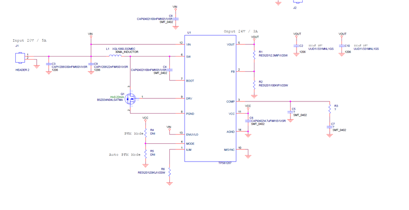
Tool/software:
Hi,
Does there have any caculator tool for TPS61287 compensation can share to us?
Or have any suggest value for Vin 20V to Vout 24V/3A?
Please help review below schematic for Vin 20V to Vout 24V/3A application.
Thanks!
Jeff


