This thread has been locked.

If you have a related question, please click the "Ask a related question" button in the top right corner. The newly created question will be automatically linked to this question.

BQ25756:How to initialize charging?

Part Number: BQ25756
Other Parts Discussed in Thread: USB2ANY, EV2400

Tool/software:

Hello, I am using the BQ25756, which communicates with an ESP32 in standalone mode. I am facing two issues that are not functioning as expected:

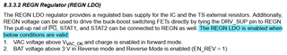
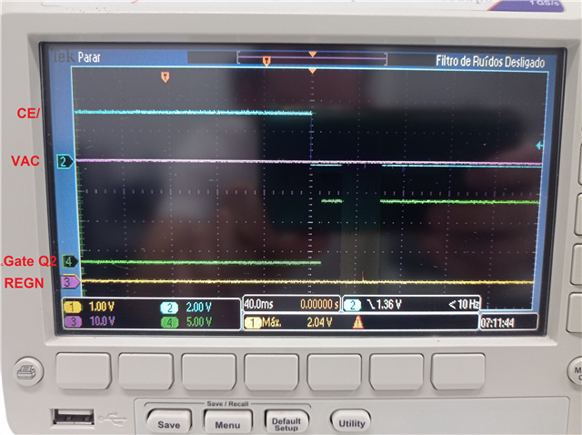
  1. The input voltage is within the operational window (38V–60V). It was verified that the PG_STAT bit is being read as 1, and the CE/ pin is pulled LOW. Using hardware, it was confirmed that the voltage on this pin is 0V, and the EN_ICHG bit is being read as 1. However, the device is still not initiating charging, and the REGN pin remains at 0V.

  2. The ADC converter seems to perform only a single conversion upon power-up and does not convert further. The procedure for reading was as follows:

    • The ADC configuration was left unchanged, using the default settings (one-shot mode, 13-bit effective resolution, etc.).
    • Conversion was enabled by writing 0x1 to ADC_CONTROL.
    • Sequential reads were performed on the registers IAC_ADC, IBAT_ADC, VAC_ADC, VBAT_ADC, and TS_ADC.
    • The values read were converted into their respective parameters according to the range specified in the datasheet, and the loop restarted at the first step (enabling the converter).

    During testing, I added a check for the ADC_CONTROL bit to verify that it was enabled, and it was indeed being read as 1. However, the ADC_DONE_STAT bit was always read as 0, indicating that the conversion had not completed. Even when waiting approximately 1 second to allow for conversion, it still failed to convert. When the verification was removed and the loop was allowed to run continuously, the ADC still did not perform any conversion, even after waiting for over 1 minute.

  • Hello Murilo,

    Thanks for working on this. I've got a few questions to help us troubleshoot this.

    1. Can you read the status and flag registers of the BQ25756 and send them to me?

    2. I haven't seen this problem before. What's the voltage on REGN here? REGN needs to be 5V for the ADC to run.

    Is there anything else you can tell me about the circuit?

    Best Regards,
    Ethan Galloway

  • Hello Ethan!

    I have some updates and additional questions to share:

    1. I noticed that pins 32 and 33 were not connected. After connecting them, the ADC converter seems to be working correctly. However, charging still does not start, even though EN_CHG=1, PG_STAT=1, and the CE/ pin is pulled LOW. Is there anything else that needs to be checked or configured to initiate charging?

    2. Even with the ADC reading the input, the REGN pin is not enabled (it remains at 0V).

    3. During testing, I noticed that a fault (TS_STAT=0x4) might be preventing REGN from generating voltage. In this case, the value read from TS is 0x0 (the default value). If the device enters a fault condition, should REGN remain at 0V, or does it stay at 5V? What are the conditions required for REGN to generate voltage?

      • I suspect, but am not certain, that if REGN does not generate voltage, it is not possible to read TS (which would result in the default reading). If this is the case, what could be disabling REGN?
    4. Does the CE/ pin need to remain LOW to stay enabled and HIGH to disable, or is a pulse sufficient to turn it on? (In my case, I keep it LOW to stay enabled and switch it to HIGH when I want to disable it. Please confirm if this method is valid).

  • Hello Murilo,

    1.

    Is there anything else that needs to be checked or configured to initiate charging?

    Here's the requirements for the device to start charging:

    2. Can you measure the voltages on VAC, VBAT and REGN?

    3.

    What are the conditions required for REGN to generate voltage?

    Here are the conditions for REGN to turn ON:

    4. Yes, the CE pin needs to remain LOW to charge. A pulse will not work.

    I've got a few questions to help debug this:

    • Can you send me your board schematic?
    • Is the load on VBAT a battery or an E-load?
    • Can you send me the charger's status registers?

    Best Regards,
    Ethan Galloway

  • Hi Ethan, thanks for the response!
    1.	
    1.1	OK.
    1.2	OK.
    1.3	The voltage at REGN is at 0V, which is why I believe it is not enabling charging, but I don't know why REGN is at 0V.
    1.4	OK.
    1.5	Failure at TS_STAT=0x4, which I believe is related to REGN being disabled, producing maximum temperature value in the reading.
    2. Yes, VAC and VBAT are read correctly by the converter even with REGN at 0V (read via multimeter).
    3. In my case I am using the BQ25756 only to charge Li-Ion and LIFePO4 batteries, I do not use the reverse mode. Is REGN LDO enabled when conditions 1 AND 2 are valid or when 1 OR 2 is valid? In my case, condition 1 is true while for condition 2 BAT is above 3 V but reverse mode is not enabled (I will just charge the battery).
    4.	
    4.1	Attached are some considerations:
      4.1.1	32 and 33 are connected now.
      4.1.2	I am not using REGN to drive DRV_SUP, in this case I am using an external 10.6V source (J4) that will also feed another board with the standalone ESP32 used to communicate with the IC.  
      4.1.3	J7 communicates with the ESP32.
    4.2	The load on the VBAT is a battery, but I also tested without a battery and the problem remained the same. Is it possible to test without a battery, in this case just leaving it empty, in which case what do I expect to happen?
    4.3	At the moment I'm not in the laboratory to obtain this data, but what I can say is that when sending LOW to CE/ (considering the other conditions for starting loading established) the only failure returned is TS_STAT=0x4, in this case TS_ADC read as 0x0 .
     Impressão-Esquemático-Potência (2).pdf
  • Hello Murilo,

    Your welcome. Thanks for being patient with this. We are busy at the moment and I'll get back to you tomorrow.

    Best Regards,
    Ethan Galloway

  • Hi Ethan,

    Ok, I’ll take this opportunity to share a few more observations:

    Attached is an image captured via oscilloscope showing the input voltage (purple), CE/ pin (blue), Gate on the MOSFET Q2 of the reference (LODRV1), and REGN. Notice that when enabling charging by pulling CE/ to LOW, the REGN remains disabled, while the gate of Q2 is enabled. Could the gate being enabled even with REGN at 0V indicate an error, or is this behavior expected? If it is an error, what could be the possible issue and the potential solution?

  • Hello Murilo,

    2.

    Yes, VAC and VBAT are read correctly by the converter even with REGN at 0V (read via multimeter).

    Can you tell me what the voltage on VAC, VBAT, DRV_SUP, FB, and REGN is? A multimeter measurement will be fine here.

    3.

    Is REGN LDO enabled when conditions 1 AND 2 are valid or when 1 OR 2 is valid?

    It's 1 OR 2.

    4.

    Is it possible to test without a battery, in this case just leaving it empty, in which case what do I expect to happen?

    Yes, this is possible. If there's no battery connected, VBAT should rise to the battery charge voltage. Then, the BQ25756 will terminate charging, VBAT will fall, and then the BQ25756 will start recharging. By the way, we have an FAQ for the BQ2575X family that goes over this.

    Here are my suggestions for the schematic:

    • I see that the threshold voltage for the FETs is really high. It ranges from 2V to 4V. This shouldn't be a problem because you have an external gate drive supply, but do you see a difference if you switch to FETs with a lower VTH?
    • I recommend installing a small ceramic cap on the node between Q3 and R2. A 1µF cap here will help filter out high frequency noise. I recommend the same thing for the VAC side as well. I don't think this is the root cause of the problem though.
    • If possible, can you send me the layout also?

    I have a few testing suggestions:

    • If possible, could you attach an EV2400 or a USB2ANY to the BQ25756? This may make testing easier.
    • Can you send me the BQ25756 register file?
    • What do the status register report while the device is trying to charge?

    Best Regards,
    Ethan Galloway

  • Hi Ethan,

    I resolved my issue with voltage generation at REGN by assembling another identical board. It was likely a hardware assembly problem that I couldn’t identify. Nevertheless, I’ll review your suggestions and attach the layouts in case you think you can make any relevant contributions.

    Let me provide some context to help you understand the nature of my project. I’m using the BQ25756 to charge Li-Ion or LiFePO4 batteries (optimized via software) with a capacity of 48V/20A. Its operating range is from 38V to 60V, with a charging voltage of 58.4V and input and charging current limits of 20A, all defined by resistors. For initial testing, I’m using a 2A battery, so I’ve programmed the IAC_DPM and ICHG_REG registers to match this value.

    Before testing with the battery, I performed a no-load test on the output, with nothing connected to it. Upon enabling charging, only PG/ and STAT1 turned ON, indicating good input power and the start of charging (CHARGE_STAT indicated trickle charging). Based on this, I have a few questions to ensure the procedure is being performed correctly:

    1. During the open-circuit output test, I noticed that the output voltage stabilized at approximately 1.1V (I monitored it for a short period, less than a minute). In this case, what behavior should I expect? I understand it’s in trickle charge mode, but I’m unsure about the expected voltage and duration during this phase. Could the observed value be correct?

    2. Since I’m adjusting the registers for a 2A battery, I also changed EN_PFM=0 and set ITERM to 250mA (the closest value to 10% of the charging current). Are these changes necessary? Are these values appropriate? Is there any other register I need to adjust?

    3. Considering that the battery to be tested is nearly fully charged (around 54V), what behavior should I expect in terms of output and input readings and the duration of the process? Do I need to define the duration of each charging stage via software?layout-Superior-Potência.pdflayout-Inferior-Potência.pdf

  • Hello Murilo,

    I'm glad to hear REGN is working now.

    In this case, what behavior should I expect? I understand it’s in trickle charge mode, but I’m unsure about the expected voltage and duration during this phase. Could the observed value be correct?

    I would expect the output voltage to rise up to the battery charging voltage (58.4V) here. Can you measure the voltage on VBAT and VFB? (To measure VFB, I'd recommend disabling charging, putting the probes on VFB, and then enabling charge again)

    What do the status and flag registers say?

    Since I’m adjusting the registers for a 2A battery, I also changed EN_PFM=0 and set ITERM to 250mA (the closest value to 10% of the charging current). Are these changes necessary? Are these values appropriate? Is there any other register I need to adjust

    Yes, these registers are appropriate. The hardware setting will also set the termination current to 10% of the charge current by default. So, you don't need to set ITERM.

    Considering that the battery to be tested is nearly fully charged (around 54V), what behavior should I expect in terms of output and input readings and the duration of the process? Do I need to define the duration of each charging stage via software?

    You should expect the charger to enter into fast charge mode and then transition to taper charge once the VFB voltage reaches VFB_REG, 1.536V by default. The battery voltage equals the charge voltage here.

    The charging stages are based off of the voltage of the battery. So, you don't need define the duration of each stage.

    Best Regards,
    Ethan Galloway

  • Hello Ethan,

    I followed the requested testing procedure and observed some strange behavior: when enabling charging (with the 2A battery already connected), it indicated a battery overvoltage fault vbat_ov_stat=1, while cv_tmr_stat=ts_stat=vac_uv_stat=vac_ov_stat=ibat_ocp_stat=tshut_stat=chg_tmr_stat=drv_okz_stat=0. The VBAT was approximately 53V, although the charging voltage was set to 58.4V (for a 48V battery), and FB measured around 51V.

    In my case, I am programming Vfb_regn to 1.544V via software and configuring the charging voltage (58.4V) using resistors of 249kΩ (Rtop) and 6.8kΩ (Rbot). In this scenario, VFBG was not generating a voltage, so I initially suspected that the FBG pin was not connected. Upon verification, everything appeared correct. To further troubleshoot, I connected two diodes in series from FBG to GND to generate a reference for FB. As a result, a voltage of approximately 1V was observed at FB, and the fast charge phase (CHARGE_STAT=3) was indicated. However, the current remained nearly zero at both input and output, and only Q2 and Q4 were switching (in this test, the input and output voltages were approximately the same).

    Despite this, the ADC readings for both input and output voltages were performed correctly. Given this behavior, I have the following questions:

    1. Is this behavior expected? What could be the reason the battery is not drawing current?
    2. Does this behavior indicate a malfunction in the IC (e.g., damaged or faulty)?
    3. What can I test at the software and hardware levels to better identify the issue?
    4. Why is the charger not charging even though the register indicates the correct charging stage?
    5. Why, with 51V at FB, is the ADC reading correct? Specifically, what does it use to measure the output voltage, and what determines the programmed charging voltage?
    6. Which voltage parameters can be programmed via software?
  • Hello Murilo,

    I'm looking at your layout and I have a few suggestions:

    • I recommend using a kelvin connection to the sense resistors for ACN/ACP and SRN/SRP. You might be able to route these traces on the back side of the board to get more room for the connections?
    • I recommend moving the VFB voltage divider (R28 and R27) closer to the IC.
    • It's hard to tell from the layout pdf file, but are the gate drive and SW traces at least 20mills wide? We recommend a width of at least 20mils for the gate drive and SW traces.
    • I would also make sure to route HIDRV1 and SW1 next to each other. SW1 is the return path for HIDRV1. I recommend the same thing for HIDRV2 and SW2.
    • Here's the BQ25756 Schematic/Layout checklist just for reference.

    For your questions:

    1. This is not expected behavior.

    2. I think either the IC is damaged or the layout is causing this issue. Could you try resoldering the FBG pin just to make sure that pin attached?

    3. See my comments below
    4. I'll need more information for this.
    5. Now that REGN is working correctly, the ADCs are probably working better now. Keep in mind that the ADCs are intended as a general indicator and we don't provide a spec for accuracy. The voltage ADCs are also more accurate at high voltages.

    6. VFB, ACUV_DPM, and the reverse output voltage can be programmed by software.

    Here are my questions to help troubleshoot this:

    • You only see Q2 and Q4 switching? There's no switching on HIDRV1 or HIDRV2?
    • What does the waveform of SW1 and SW2 look like?
    • To add on to that, what does the waveform on VFB and VBAT look like? Once again, be careful when putting probes on VFB.
    • If possible, can you reflow the IC? Does this change the behavior?

    Best Regards,
    Ethan Galloway

  • Hello Ethan,

    I’m reviewing your suggestions. Regarding the questions:

    1. Ok.
    2. The FBG pin was connected directly to GND. Is there an issue with this?
    3. Ok.
    4. What I mean is that the status register (charge_stat) correctly indicates the stage the charging process should be at based on the output voltage (for example, when I connect the 53V battery, it indicates fast charging, but it is not actually charging). In this case, it seems that the system does not verify whether the switching is happening correctly for this stage; it only relates the status to the output voltage.
    5. Ok.

    6.1. Yes, only Q2 (yellow) and Q4 (blue) are switching, while Q1 (purple) and Q3 (green) are not switching correctly, as can be seen in "attachment6.1".

    6.2. In "attachment6.2", the waveform for SW1 (blue) and SW2 (purple) is shown compared to the gate of Q2 (yellow).

    6.3. In "attachment6.3", the VFB (blue) and VBAT (purple) are shown compared to the gate of Q2 (yellow). Unlike the previous tests that were done with no load, in this test, both the input and output were supplied with approximately 43V.

    6.4. The IC has been reflowed and it has been confirmed that all the pins are properly connected.

            7. It is observed that the capacitors C1 and C2 are not charging, which seems to be influencing the ramp waveform (instead of a square one) on the gates. What could be the cause of this, and what is a possible solution?

    AnexosTI.zip

  • Hello Ethan, I have new information to add for your analysis. Thank you in advance:

    1. In a recent test, the SE100150G MOSFETs were replaced with the IRF540N model to evaluate whether the switching response times improved. In "NewQ," we observe the readings for the lower switches (blue and yellow) and the upper switches (green and purple) after these replacements. Indeed, compared to the previous results, the response times are faster. However, the upper switches are still not being activated. What can you tell me about the behavior of the gate signals and the potential need for a MOSFET replacement?

    2. In the new measurement, it was verified that the lower switches are operating, and capacitors C1 and C2 are charging. Additionally, it was observed that the gates of Q1 and Q3 exhibit a constant voltage of 1V (Q3 appears to be attempting to switch, or it might be noise from the probe). The conclusion is that the lower switches and the charging of capacitors C1 and C2 are working as expected. However, for some reason, it seems that the IC is not driving the BTST1/2 voltage to HDRV1/2. This is despite DRV_SUP being externally powered at approximately 10.6V, while only about 1V is reaching HDRV1/2. Also, note that during these tests, the input and output voltages were approximately 43V. Under these conditions, what behavior should I expect from the switches?

    3. In summary, the lower switches seem to be functioning correctly, and capacitors C1 and C2 are charging. However, the IC, through HDRV1/2, is not providing sufficient voltage to activate the upper switches, even though DRV_SUP is being powered at around 10.6V.
      10.1. Have you encountered this type of issue before?
      10.2. It appears that the peripherals connected to the IC are working, but the IC itself does not seem to be functioning correctly as it fails to drive the upper MOSFETs. Is this assessment accurate? How can I diagnose whether the issue lies with the IC itself or some other condition? (Keep in mind that the IC is communicating with the interface and performing ADC readings correctly).
      10.3. Regarding the four switches, what behavior should I expect when charging begins under the following conditions: VAC > VBAT, VAC < VBAT, and VAC = VBAT?

  • Hello Murilo,

    Thanks for being patient with this. I'll get to your most recent questions tomorrow.

    Best Regards,
    Ethan Galloway

  • Hello Murilo,

    2. There should not be a problem with connecting FBG directly to GND.

    4. Thanks for clarifying this.

    6. Thanks for images.

    7. C1 and C2 not charging shouldn't influence the LODRV gate traces

    8.

    What can you tell me about the behavior of the gate signals and the potential need for a MOSFET replacement?

    At the current moment, I think trying out different FETs with a lower VGS and a lower COSS would be good.

    9.

    Also, note that during these tests, the input and output voltages were approximately 43V. Under these conditions, what behavior should I expect from the switches?

    You should see SW1 and SW2 interleaved together. SW1 and SW2 will be switching at 1/2 FSW.

    10.

    10.1. Have you encountered this type of issue before?

    I have not encountered this type of issue before.

    but the IC itself does not seem to be functioning correctly as it fails to drive the upper MOSFETs. Is this assessment accurate? How can I diagnose whether the issue lies with the IC itself or some other condition?

    I think the issue lies with the circuitry around the IC.

    10.3. Regarding the four switches, what behavior should I expect when charging begins under the following conditions: VAC > VBAT, VAC < VBAT, and VAC = VBAT?

    VAC>VBAT - Buck Mode - Only SW1 will be switching

    VAC<VBAT - Boost Mode - Only SW2 will be switching

    VAC = VBAT - Buck Boost Mode - SW1 and SW2 will be switching at 1/2 FSW.

    I have a few more testing suggestions:

    • I see the DCR of the inductor is only 2.86mΩ. Do you see any change if you change the inductor to an inductor with a higher DCR?
    • I also see the threshold voltage of the switching FETs is 4V. This should be fine because the circuit has a 12V gate drive supply, but do you see any difference if you change to FETs with a VGS of around or under 2V?
    • Does the IC behavior change if you use REGN for DRV_SUP?

    Best Regards,
    Ethan Galloway

  • Hello, Ethan,

    Thank you again for your clarifications. Regarding your question: "Does the IC behavior change if you use REGN for DRV_SUP?", I have a doubt. In my case, I am not using REGN to drive the MOSFETs but rather an external power supply of approximately 10.6 V that feeds DRV_SUP, as shown in the schematic.

    However, the REGN and DRV_SUP pins are not connected in my setup. Are you suggesting that the same power supply used for DRV_SUP could also be used to feed the REGN pin (in this case, connecting REGN and DRV_SUP)? Considering the supply voltage is around 10.6 V, could this cause any issue in the circuit?

    It is worth mentioning that I previously tested connecting DRV_SUP to REGN, but in that case, the circuit could not even drive the LEDs. However, during that test, there was no 10.6 V power supply feeding both pins.

    I look forward to your guidance.

  • Hello Murilo,

    Thanks for catching this. Please don't connect 10.6V to REGN.

    It is worth mentioning that I previously tested connecting DRV_SUP to REGN, but in that case, the circuit could not even drive the LEDs. However, during that test, there was no 10.6 V power supply feeding both pins.

    Thanks for the information here.

    Also, can you read the I2C registers of the device? What do the status and flag registers say while trying to charge?

    Best Regards,
    Ethan Galloway

  • Hello Ethan,

    Alright, 10.6V and REGN are not being connected, and moreover, a new layout incorporating the suggested recommendations is being prepared.

    The status registers seem to be indicating correctly based on the output voltage. For instance, when no battery is connected, it indicates slow charging, and with a battery at 53V, it indicates fast charging. However, in neither of these cases is the output actually being charged.

  • Hello Murilo,

    Thanks for the information about the registers. If possible, can you send me the register file?

    Have you tested an inductor with a higher DCR yet?

    Also, your schematic appears to show an inductor with a center tap and the center tap is connected to PGND. Just to be sure, the inductor isn't connected to GND at any point right?

    Best Regards,
    Ethan Galloway

  • Hello Ethan,

    The inductor used (MTP2918E-100M-H) does not have a center tap. The third terminal shown in the schematic is labeled as 'N/C' in the datasheet and has been connected to GND solely to enhance thermal dissipation.
    The new layout is currently being prepared.

  • Hello Murilo,

    Thanks for the new information. Let me know how the new layout performs.

    Best Regards,
    Ethan Galloway

  • Hello Ethan,

    The new layout has been designed incorporating the suggested changes. Progress has been made, as capacitor C2 is now charging; however, the gate of switch Q1 is not switching—it remains at a constant high voltage—causing a short circuit and resulting in Q1 burning out (while the other switches are operating correctly).

    It has been considered that the IC might not be functioning properly, although I find this possibility unlikely.

    What do you suggest could be causing the malfunction? Additionally, what further tests can be conducted to diagnose the issue?

  • Hello Murilo,

    That is strange. Why would Q1 be high all the time?

    I've got a few questions to help us debug this:

    • What voltages does this problem occur at?
    • Do you see a difference in the behavior if you go to an inductor with a higher DCR? 11mΩ would be optimal to test. This is same DCR that the EVM has.
    • Have you performed an ABA swap on the IC to see if the behavior follows the IC or the board?
    • Can you send me your updated layout?

    Best Regards,
    Ethan Galloway

  • Hi Ethan,

    The IC has been replaced, but testing has not yet been performed, so I am unable to provide an update at this time. The inductor issue is also under investigation.

    Attached, you will find the layout and schematic of the new project for your review.layoutsS.zip

  • Hello Murilo,

    Thanks for the updated information. I'll review the layout later this week and get back to you.

    Best Regards,
    Ethan Galloway

  • Hello Murilo,

    The updated layout looks good. I have one other suggestion for the layout. Make sure ACN/ACP and SRN/SRP connect directly to the sense resistor pins (R1 and R2) without going through a trace that might carry high current. This will improve the accuracy of these control loops.

    Also, for the current behavior you are seeing, can you send me the registers?

    Let me know what your further tests show

    Best Regards,
    Ethan Galloway