This thread has been locked.

If you have a related question, please click the "Ask a related question" button in the top right corner. The newly created question will be automatically linked to this question.

LM2596: Analyze the rationality of the circuit diagram

Part Number: LM2596

Tool/software:

1、Below is our circuit diagram

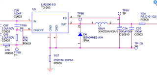
2、We have some product failures and the output voltage of the DCDC chip is 3.7V.

3、I would like to ask if it is caused by inductor L1. The actual inductor used is 47uH, and the rated current is 1.55A.However, the datasheet of TI recommends 33uH, and whether its rated current must meet 3A, when the actual power consumption of my back end is only 200mA.

4、The GND pin of the chip is connected in series with the magnetic bead PB7, whether it will elevate the GND pin voltage and cause the 1.235 reference voltage inside the feedback pin to decrease, thus pulling down the output voltage to 3.7V.

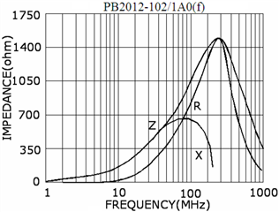
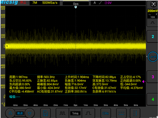
5、The following is the characteristic curve diagram of the magnetic bead and the voltage waveform diagram between the low voltage negative electrode and the GND of the PCB.

6、Thank you very much!

  • Hello,

    There should not be anything connected between the IC GND pins and the GND plane of the PCB. Remove the bead and make a direct connection to GND. 

    The configuration you have does not allow for proper grounding and may cause the device to behave abnormally. 

    Use the recommended inductor and make sure that it is rated for the high side current limit of the device.

    Make sure to follow all of the datasheet recommendations in your design.

    Best regards,

    Ridge

  • Hello,

    I am closing this thread due to inactivity.

    Best regards,

    Ridge