This thread has been locked.

If you have a related question, please click the "Ask a related question" button in the top right corner. The newly created question will be automatically linked to this question.

TPS61235P

Part Number: TPS61235P
Other Parts Discussed in Thread: BQ24170,

Tool/software:

We have a product that is essentially a USB battery pack - it's a large 99Wh lithium ion battery pack, charged via 5v USB using a BQ24170 charge IC.

The output is boosted from the lipo back up to 5V using a TPS61235.  We've had a high number of failures in the field with these devices, around 12-15% from a sample set of around 500 so far.  We test them in house extensively before they leave our facility, and have torture tested them internally beyond the boost current levels we'd typically see in the field, and had no issues.   Board layout is as indicated below.  When the devices are returned, 5v applied to EN no longer creates any signal or voltage on +5v out.  We swap the TPS61235 on the board and normal service is restored.
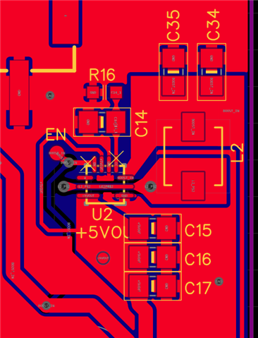
C14 - .1uf

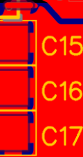
C15, C16, C17 - 22uf

C34 - 1uf

C35 - 10uf

L2 - 1uH

R16 - 33k

When scoping a normally functioning device, SW signal shape looks reasonable given my sub-optimal probes.  Failed devices appear to be shorted to VDD and show battery voltage on the SW node.

What are my next steps on understanding this issue?

  • Hi Christopher,

    The layout is not good enough, which may causes overvoltage stress on low side MOSFET . Please measure the impedance between SW to GND on failed parts. If the SW is short to GND on failed parts, then most likely the issue is caused by switching ringing on SW pin.The solution is to reduce parasitic inductance around Cout.current loop.

     My advise is, place C15 close to the IC as possible. and do not use cross connection on GND polygon pour (C15-17 and IC GND pin)

    Best Regards,

    Travis

  • Is it possible to understand under what conditions this is most likely to cause an issue?  i.e., quiescent, fully loaded, at load connect or load disconnect, etc?

    Could you clarify "do not use cross connection on GND polygon pour (C15-17 and IC GND pin)".  

    Could an underrated inductor contribute to this issue as well?  We chose an inductor rating of 4.5A which seemed sufficient when the design was created, but the more I understand SW currents perhaps this is also underrated for our net 2.5A boost output.

    Travis - thank you!  I really appreciate your input here.

  • Hi Christopher,

    [Q] Is it possible to understand under what conditions this is most likely to cause an issue?  i.e., quiescent, fully loaded, at load connect or load disconnect, etc?

    [A] Heavy load and High Vout (caused by load disconnect overshoot)

    [Q] Could you clarify "do not use cross connection on GND polygon pour (C15-17 and IC GND pin)".  

    [A] It should be called relief connect in Altium. I mean we recommend direct connect 

    [Q] Could an underrated inductor contribute to this issue as well?  We chose an inductor rating of 4.5A which seemed sufficient when the design was created, but the more I understand SW currents perhaps this is also underrated for our net 2.5A boost output.

    [A] No, this issue is not related with inductor

    For more understanding about this type of layout issue, you can look at this article. This APP note is not based on TPS61235P parts but the layout consideration applies for all boost converters

    TPS61022 and TPS61023 Boost Converters Layout Guidelines

  • Understood.  We will update these layouts for future runs and hope this improves our results.

    That said, I find no evidence of a short to ground on SW, so I hope the root cause isn't being misunderstood.

    When a failed module is powered, I see constant DC Vbatt on the SW pin.  Does this imply anything different from what's been covered already?

  • Hi Christopher,

    The layout issue is confirmed and this will arouse reliability issue sooner or later. But if SW is not short to GND, then there might be some other problems. Can you catch waveform of Vin SW and Vout on failed parts when the Vin is applied? And use DC voltage source on Vin to test the leakage current.

    Best Regards,

    Travis

  • Here is a revised layout for review.

  • Also, here are the SW, Vin(Vbatt), and Vout traces on battery connect.

    Yellow is SW, Green is Vbatt, and Purple is Vout.  

  • Hi Christopher,

    About new layout:

    Please use direct connect on these pads. Other parts are good.

    About waveform:

    Is the EN signal high in this waveform?

    Best Regards,

    Travis