BQ76952: BQ7695204 Problem with ADCIN functionality on multipurpose pins

Part Number: BQ76952
Other Parts Discussed in Thread: EV2400,

Tool/software:

Hello,

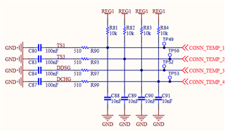
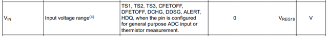
I am trying to read temperatures from the TS1, TS3, DCHG and DDSG pins. They are connected to an external thermistor, and I checking with a multimeter I can read voltage in the pin. However, I cannot get a valid measurement from the device. 

First of all, I tried to read the pin voltage by configuring the pins as ADC inputs:

TS1 Pin Configuraiton = 0xB3

TS3 Pin Configuraiton = 0xB3

DCHG Pin Configuraiton = 0xB3

DDSG Pin Configuraiton = 0xB3

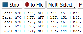
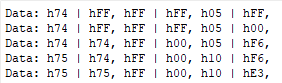
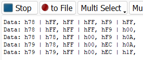
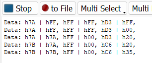
But I only get a valid voltage measurement from TS1 (Command 0x70). All the other ones are reading 0.

Then I tried to configure them as Thermistors, with the 18K Temperature Model: Config = 0x0B. With this configuration, I read a constant value of 1890. 

I also found a document that mentions that with this configuration of the 18K Temperature Model:
– A1 = 0, B1 = 0, A2 = 0, B2 = 0, A3 = 0, B3 = 32767, A4 = 0, B4 = 0, A5 = 16384, Adc0 = 11703

I can get also raw ADC measurements with the Thermistor configuration, but again I still read a constant value of 1535. Even if I check the DASTATUS7 I find no counts at all.

What am I missing? is there some other configuration that I am forgeting to set? I find strange that TS1 works well as ADC input while all the other ones do not.

Any help will be appreciated. 

  • Hello Federico,

    Do you mind sharing your schematic showing the connections at those pins? I see you have them configured for ADCIN functionality. Do you have any of your own pull-ups you are using for your thermistors?

    Best Regards,
    Alexis

  • Hello Alexis,


    Thanks for replying! Here is a schematic of the connections at those pins:

    The thermistors would be connected at CONN_TEMP_X

  • Hi Federico,

    What voltage is being applied to the pins? The recommended range for ADCIN mode is between 0~1.8V:

    If you have an EV2400 available, I suggest connecting it to the board to see if there is an issue with the readout.

    Regards,

    Max Verboncoeur

  • Hello Max,

    Thanks for your reply. The voltage being applied to the pins is within the range you mentioned. I am using the same thermistors connected in the same manner to TS1, TS3, DCHG and DDSG. Only TS1 reads correctly the voltage, all the other ones are measuring 0 as ADCIN. If I measure with a multimeter, I can see around 1,6 V on those pins.

    Unfortunately, I do not have an EV2400 available.

  • Hello Federico,

    From what you have shared, it seems there is a chance the configuration you set didn’t apply/isn’t applying. Can you check the configuration settings for those pins again to see if they are properly set to ‘0xB3’?

    Best Regards,
    Alexis

  • Hello Alexis,

    Sorry for the delay. I have checked and the configuration settings for those pins is correct. I read the same value I programmed: 0xB3.

    Here is a summary of the current situation:

    - TS1, TS3, DDSG and DCHG are all configured as ADCIN, with value 0xB3. I've checked after setting the configuration and the values are properly set in the memory.

    - Voltage in REG18 is 1.83 [V]

    - Connected to CONN_TEMP_X (see schematic in previous message) I have the same thermistors for each pin.

    - Measuring with a multimeter, I can see all pins have the same reading, around 1.7 [V].

    TS1 measures correctly the voltage in ADCIN functionality, but the other three pins measure 0 [V].

    Best regards,

    Federico

  • Hello Federico,

    Thank you for double checking the configuration settings and summarizing the situation.

    Are you reading the ADCIN voltages through the 0x70, 0x74, 0x78, and 0x7A commands as well or are you using different commands?

    Do you mind sending a logic analyzer file of you sending the commands to read the voltages for TS1, TS3, DCHG, and DDSG?

    Do you also have an EVM you are using?

    Best Regards,
    Alexis

  • Hello Alexis,

    Yes, I am using the 0x70, 0x74, 0x78, and 0x7A commands to read the ADCIN voltages. I've also tried to read the DASTATUS 6 and 7 to get the raw counts, but they show the same issue: TS1 reports some counts but the other 3 show 0.

    I've used a Digital Analyzer to monitor the SPI communication during these commands. Here is what I got for each of them:

    (in case you are not familiar with WaveForms, each line represents an SPI transaction (CS high->low). Within it, each byte transaction is displayed in a pair ( x | y ), where x is the byte in the MOSI and y is the corresponding byte in the MISO)

    0x70 (TS1, the one that measures correctly)

    for example, here there are three pairs of bytes. The first pair is the command (0x70), the second one is the data (0xFF means I don't care since I am reading data in this case), and the third pair is the CRC.

    0x74

    0x78

    0x7A

    Unfortunately, I do not have an EVM available. I am using the BQ76952 in a customized board.

    Best regards,

    Federico

  • Hello Federico,

    Do you mind sharing your entire schematic? If you would like to keep it private, you can DM it to me instead as well.

    Best Regards,
    Alexis

  • Hello Federico,

    Thanks for sharing your schematic. Please give me some time to review it.

    Do you mind sending me a logic analyzer file of you configuring TS3, DDSG, and DCHG as an ADCIN as well and then reading the RAM registers of the configurations? Are you also going into CONFIG_UPDATE mode to make these changes? 

    Best Regards,
    Alexis 

  • Hello Alexis,

    Somehow, I was able to briefly read those pins correctly. I say briefly because the behavior seems to be erratic. The same code I use to program the registers does not yield the same results every time. So, seems that the problem here is a software one (which is some relief). Can you give me some advice on what is the correct procedure to put the device into config mode and write the ram registers with my desired configuration? Should I add delays between each ram register write operation? Is there a prefered order I should configure the registers? 

    Have you noticed anything in the schematic that could be causing issues?

    Best regards,

    Federico

  • What drives the MISO pin? I've noticed that when I power up the system, the MISO line is always low and there is no voltage in REG1. I then send a reset subcommand to the device and after that, the SPI starts working fine and there is voltage in REG1. I then go into config mode, start writing the ram registers, but after I send the subcommand to exit config mode, the MISO is again kept low during SPI communications and there is no voltage in REG1.

  • Hello Federico,

    That’s good to hear that you were able to briefly read those pins correctly even if it doesn’t seem to be consistent yet.

    Can you give me some advice on what is the correct procedure to put the device into config mode

    To put the device into CONFIG_UPDATE mode, you need to use the subcommand 0x0090 SET_CFGUPDATE and follow the steps as shown in Figure 5.3 Subcommand Example: Device Number – 0x0001 of the BQ769x2 Software Development Guide. To exit CONFIG_UPDATE mode, the subcommand is 0x0092 EXIT_CFGUPDATE.

    Should I add delays between each ram register write operation?

    We recommend using a 2 ms wait time after writing to 0x3E/0x3F before reading the result from the transfer buffer for subcommands. This is explained a bit more in Section 2 Subcommands of the Software Development Guide.

    Is there a prefered order I should configure the registers

    There also isn’t a preferred order to configure the registers.

    What drives the MISO pin? I've noticed that when I power up the system, the MISO line is always low and there is no voltage in REG1. I then send a reset subcommand to the device and after that, the SPI starts working fine and there is voltage in REG1. I then go into config mode, start writing the ram registers, but after I send the subcommand to exit config mode, the MISO is again kept low during SPI communications and there is no voltage in REG1.

    What is the specific part number you are using? Depending on the part number, the REG1 LDO may or may not be enabled by default. Section 5 Device Comparison Table on the datasheet shows the various versions. Something to also check is the Settings:Configuration:SPI Configuration. This configures the SPI MISO pin to use REG1 or 1.8V.

    Have you noticed anything in the schematic that could be causing issues?

    The schematic looks fine so far. 

    Best Regards,
    Alexis