This thread has been locked.

If you have a related question, please click the "Ask a related question" button in the top right corner. The newly created question will be automatically linked to this question.

LM5118: Buck-Boost converter output becomes unstable after 3 to 6 hours of operation under power-on conditions at 55°C.

Part Number: LM5118

Tool/software:

Hello Team,

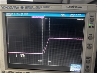
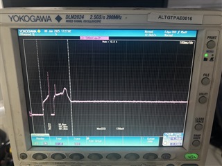
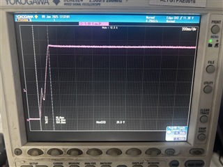
The Buck-Boost converter output becomes unstable after 3 to 6 hours of operation under power-on conditions at 55°C.

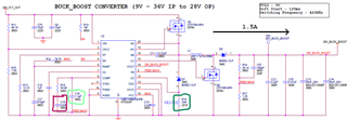
Please see the attached schematic.

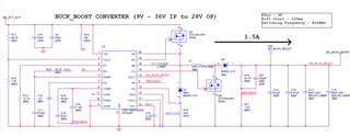
The Buck-Boost converter output becomes unstable after 3 to 6 hours of operation at 55°C, even though it continuously restarts.

Please provide solution and suggestions...

  • Hi Thirupathi,

    can you share more details e.g.:

    - waveforms (e.g. output voltage, SS, COMP)

    - does this only happen at 55 degree

    - does it happen faster a higher Temp?

    - does it never happen at lower Temp?

    - have you checked the loop stability under normal condition? What is your phase and gain margin?

    This often is related to temp dependency of external components e.g. Capacitors. Can you check them for that.

    Best regards,

     Stefan

  • HI Stefan,

    Thanks for your response

    - does this only happen at 55 degree

    Yes.

    -does it happen faster a higher Temp?

    No, we are maintaining 5C/min.

    - does it never happen at lower Temp?

    We didn't test

    - have you checked the loop stability under normal condition? What is your phase and gain margin?

    We have used the We bench design as-is. Could you guide us on how to perform the exact calculations?

    This often is related to temp dependency of external components e.g. Capacitors. Can you check them for that.

    A: Could you please provide more detailed information about that?

  • Hi Thirupathi,

    the loop stability is set by the compensation and can be calculated within some boundaries but as there are also parasitic parameters on each component and PCB this can also deviate from the math with ideal parameters.

    See also: /cfs-file/__key/communityserver-discussions-components-files/196/3678.slup340.pdf

    The best is to check and measure the loop stability on the board itself with an vector network analyzer.

    See also:

    https://www.omicron-lab.com/fileadmin/assets/Bode_100/ApplicationNotes/DC_DC_Stability/App_Note_DC_DC_Stability_V3_3.pdf

    Are all boards showing this behavior, how many have you tested?

    Best regards,

     Stefan

  • Are all boards showing this behavior, how many have you tested?

    Yes, we tested between 4 and 8 boards, but the issue still persists.

    We have total capacitive load is approximation 5200uF.

    Please see my current design values below:

    LM(2)5118 Quick Start Component Calculator Version 2.01
    Revision date: April 2014


    Step 1 - Application Requirements
    Vout (V) 28
    Enter design requirements in the shaded cells Vin(min) (V) 9
    Vin(max) (V) 40
    Maximum Average Load Current Iout (A) 1.5
    Ripple Current as % of Maximum Load Current (%) 40%
    Effciency of Converter (%) 85%
    VCCX Voltage (V) 0
    Vin at start of Transition to Buck-Boost Mode (V) 37.24
    Buck-Boost Mode Operation YES

    Recommended Controller IC LM5118

    Step 2 - Switching Frequency
    Maximum Possible Switching Frequency (kHz) 608
    Switching Frequency (kHz) 420
    Timing Resistor, Rt (kW) 12.22

    Step 3 - Inductor Value
    Calculated Buck Mode Inductor Value, Lb (µH) 33.33
    Calculated Buck-Boost Mode Inductor Value, Lb-b (µH) 27.03
    Actual Chosen Inductor Value, L (µH) 33
    Inductor Tolerance (%) 10%

    Step 4 - Calculate Output and Inductor Currents Based on Chosen Inductor
    Buck mode Ripple Current at Vin(max), ΔI (A) 0.61
    Buck-Boost Ripple Current at Vin(min), ΔI (A) 0.49
    Buck-Boost Ripple Current at Vin=Vout, ΔI (A) 1.01
    Buck mode Ripple Current at Vin(max), Including inductor tolerance, ΔI (A) 0.67
    Buck-Boost Ripple Current at Vin(min), Including inductor tolerance, ΔI (A) 0.55
    Buck Average Inductor Current at Vin(max), Including Effciency (A) 1.76
    Buck-Boost Average Inductor Current at Vin(min), Including Effciency (A) 7.25
    Buck-Mode Peak Inductor Current, Ip(b) (A) 2.10
    Buck-Boost Mode Peak Inductor Current, Ip(b-b) (A) 7.53

    Step 5 - Sense Resistor
    Current Limit Margin (% beyond Max Load) (%) 10%
    Buck Mode K Factor (K) 1.83
    Selected Buck Mode K Factor (K) 2.00
    Buck-Boost Mode K Factor (K) 2.11
    Selected Buck-Boost Mode K Factor (K) 2.20
    Current Sense Resistor, Rs (mW) 28.86
    Closest Standard Value, Rs (mW) 10.0

    Step 6 - Ramp Capacitor
    Cramp (pF) 1650
    Closest Smaller Standard Value, Cramp (pF) 330
    Rramp (kW) 78

    Step 7 - Current Limits
    Buck Mode Peak Inductor Current Limit (A) 9.97
    Buck-Boost Mode Peak Inductor Current Limit (A) 22.27

    Step 9 - Output Capacitors (Based on Worst Case Conditions for Each Mode)
    Target output ripple (mV) 50
    Buck-Boost Duty cycle at Vin(min) (%) 76%
    Buck-Boost RMS Ripple Current in Output Cap (A) 2.65
    Minimum COUT output Capacitor Value (µF) 54.05
    Required COUT ESR (mW) 7.80
    Chosen COUT output capacitor value (µF) 112
    Actual COUT ESR (mW) 10
    Buck Mode Output Ripple Voltage (mV) 64.1

    Step 10 - Input Capacitors (Based on Worst Case Conditions for Each Mode)
    Buck-Boost RMS Input Ripple Current (A) 2.65
    Buck-Boost Mode Peak to Peak Current Ripple in Input Cap (A) 7.53
    Buck Mode RMS input Ripple Current (A) 0.75
    Buck Mode Peak to Peak Current Ripple in Input Cap (A) 2.10
    Initial Input Capacitor Value(μF) 8.96
    Chosen CIN Input Capacitor Value (µF) 100

    Step 11 - Feedback Resistors
    Rfb2 (W) 26,100.00
    Rfb1 (W) 1,199.2

    Step 12 - Chb & Cvcc Capacitor
    High-side MOSFET Qg at VGS=10V (nC) 30.00
    Minimum Bootstrap Capacitor Chb (µF) 0.09
    Chosen Value for Chb (µF) 0.1
    Minimum VCC Bypass Capacitor Cvcc (µF) 1

    Step 13 - Error Amplifier Compensation
    Right Half Plane Zero Frequency (kHz) 7.039
    Capacitor ESR Zero Frequency (kHz) 142.10
    Capacitor Pole Frequency (kHz) 0.134
    Bandwidth (kHz) 1.76
    Selected Bandwith (kHz) 1.95
    Target Compensation Zero (kHz) 0.195
    Target Compensation Pole (kHz) 7.039
    Cpole (nF) 1.54
    Select Nearest Standard Cpole Value (nF) 2.2
    Czero (nF) 54.07
    Select Nearest Standard Czero Value (nF) 100.00
    Rcomp (W) 15,103
    Select nearest Standard Rcomp Value (W) 10,000

    Step 14 - Soft Start capacitor
    Choose soft-start time (ms) 123
    Soft Start Capacitor Value (nF) 1000.0

    Step 15 - UVLO Threshold and Hiccup Mode Restart
    Minimum Value of Resistor Ruv1 (kW) 40
    Chosen Value of Ruv1 (kW) 48.7
    Desired Undervoltage Threshold (V) 9
    Ruv2 Value (kW) 7.48
    Choose off-time of hiccup duty cycle (µs) 2400
    Vin voltage for desired hiccup mode off-time (V) 12
    Hiccup Mode Off-time Capacitor Value Cr (nF) 389.35

  • Hi Thirupathi,

    can you just attach the excel sheet itself. That would be easier and more efficient.

    Best regards, 

     Stefan

  • CDU_snvu065a (1).xlsm

    Please find the attached excel file.

  • Hi Thirupathi,

    in the calculator you have entered a COUT value of 112uF but above you mention an capacitive load of 5200uF.

    How do the two values correlate or how is the capacitive load connected?

    Best regards,

     Stefan

  • Hi Stefan,

    Thanks for your response.

    We have updated the design excel sheet; please go through it.

    8306.CDU_snvu065a (1).xlsm

  • Hi Thirupathi,

    Our engineer is out of office, and will return on the 7th of January. Please expect some delays in our response. 

    Best Regards,

    Feng

  • Hi Thirupathi,

    as you can see from the Gain/Phase diagrams you have only very little phase margin. So you need to adjust the compensation.

    Note: A phase margin of > 60 Degree is recommended. Less then 50 Degree is critical.

    Best regards,

     Stefan

  • Hi Stefan,

    Thank you for your response.

    Wishing you a Happy New Year!

    We have updated the latest compensation values in the Excel sheet and tested the unit, but unfortunately, the issue persists.

    Could you please suggest the values are related to the compensation to achieve the exact gain/phase margin?

    4062.CDU_snvu065a (1).xlsm

  • Hi Thirupathi,

    can you share more details e.g.:

    - waveforms (e.g. output voltage, SS, COMP) showing the instability

    Please also let me know which values you have changed compared to the schematic shown above for capturing this scope plots.

    Best regards,

     Stefan

  • Hi Stefan,

    The details have been highlighted on the schematic:

    C18=1uF, C16=10nF and Kelvin R18=18 to 20 mΩ

    Thanks & Regards

    Thirupathi T

  • Hi Thirupathi,

    I assume you will also share the requested scope plots soon.

    Best regards,

     Stefan

  • Hi Stefan,

    Please find the below attached images.

    1. SS

  • 3. Output waveform:

  • Hi Thirupathi,

    The waveform does not show the instability you have mentioned. So i assume that this is in normal operation condition.

    It also shows that in the startup phase there is an additional restart. So it looks like the softstart time is selected to short or the over current limit has not enough margin.
    Another reason would be that the input supply does dip in that phase.

    Best regards,

     Stefan