UCC21540: Minimum pulse width system-level study

Part Number: UCC21540

Tool/software:

Hi,

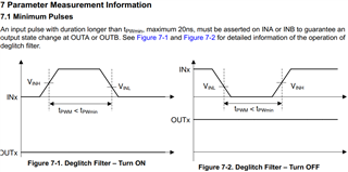
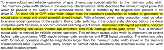
Section 8.3.4 of the November 2024 datasheet release refers to a potential risk of causing shoot-through by not adhering to a certain minimum pulse width. In addition, this minimum pulse width is dependent on many circuit parameters.

The question here is twofold:

  1. What are the System-level studies that should be carried out to determine the minimum output pulse width in a specific application?
  2. Is the shoot-through risk only because of the possible EOS driver damage during non-zero current switching events? Or is there a risk of direct shoot-through due to the output stage not changing state as indicated in section 7.1, even if there is no EOS driver damage?

  • Hi Nico,

    Thank you for reaching out!

    What are the System-level studies that should be carried out to determine the minimum output pulse width in a specific application?

    The focus should be on ensuring that there is no current in the gate loop path when the driver switches states. To do this you will need to know the charge/discharge time of the MOSFET capacitance and have the minimum ON and OFF pulse inputted to the driver be longer than these durations. 

    Is the shoot-through risk only because of the possible EOS driver damage during non-zero current switching events? Or is there a risk of direct shoot-through due to the output stage not changing state as indicated in section 7.1, even if there is no EOS driver damage?

    The EOS driver damage caused by narrow pulses typically would not cause a shoot-through. I believe that the application note is referring to the input deglitch filter that can hold the output high. This would allow both outputs to be on if deadtime interlock function is not enabled in the application.

    Hope this helps with your questions. Please feel free to ask any additional questions if needed.

    Regards,

    Hiroki

  • Hi Hikori,

    Please see below.

    The focus should be on ensuring that there is no current in the gate loop path when the driver switches states. To do this you will need to know the charge/discharge time of the MOSFET capacitance and have the minimum ON and OFF pulse inputted to the driver be longer than these durations. 

    Would you recommend measuring the Vgs rise/fall times to establish the minimum ON and OFF pulses in our specific application?

    The EOS driver damage caused by narrow pulses typically would not cause a shoot-through. I believe that the application note is referring to the input deglitch filter that can hold the output high. This would allow both outputs to be on if deadtime interlock function is not enabled in the application.

    Can you therefore confirm that if the deadtime is set via the external resistor, that it is not possible for the deglitch filter to cause shoot-through via a narrow pulse?

  • Hi Nico,

    Would you recommend measuring the Vgs rise/fall times to establish the minimum ON and OFF pulses in our specific application?

    Yes, that is the best approach to see how long it takes to fully charge/discharge. 

    Can you therefore confirm that if the deadtime is set via the external resistor, that it is not possible for the deglitch filter to cause shoot-through via a narrow pulse?

    Yes, I can confirm this. With deadtime set, there would not be instances of shoot-through caused by narrow pulses. 

    Regards,

    Hiroki