Tool/software:
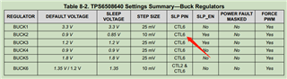
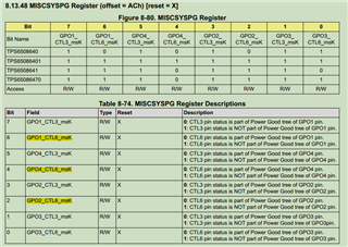
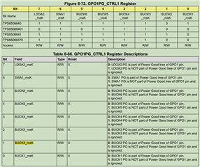
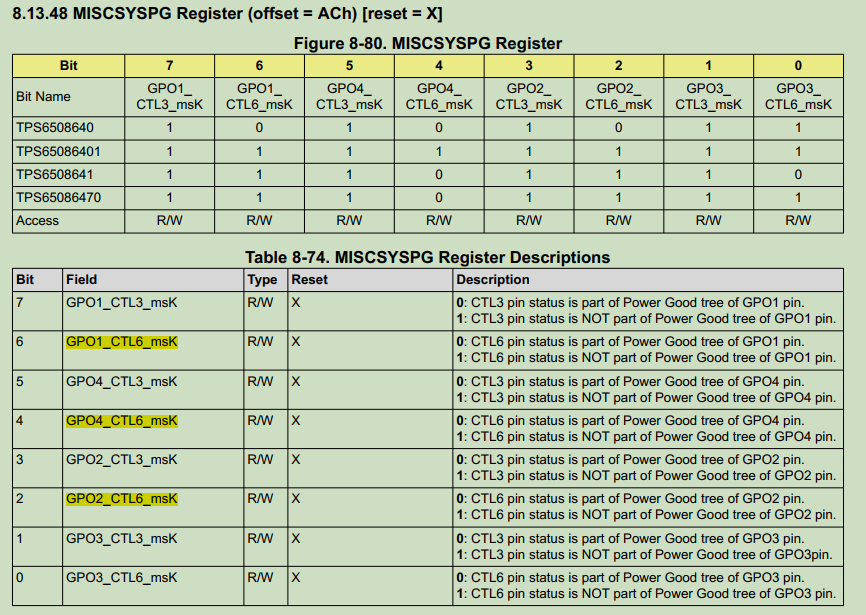
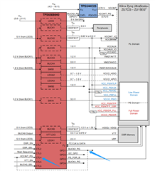
For TPS6508641, please help confirm which buck/ LDO/ switches are controlled by the power enable signals CTL1-CTL6, and which buck/ LDO/ switches are monitored by the power good signals GPO1-GPO4.
Tool/software:
For TPS6508641, please help confirm which buck/ LDO/ switches are controlled by the power enable signals CTL1-CTL6, and which buck/ LDO/ switches are monitored by the power good signals GPO1-GPO4.