This thread has been locked.

If you have a related question, please click the "Ask a related question" button in the top right corner. The newly created question will be automatically linked to this question.

TPS54519: Inquiry about PWRGD pin of TPS54519RTER

Part Number: TPS54519


Tool/software:

Hi, TI expert

I have a customer inquiry about PWRGD pin of TPS54519RTER.

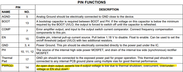
Q1) In each case of conditions that output Low: Thermal shutdown, Overcurrent, Over/Under-voltage, EN Shut down, are the Low output interval and duration the same or different?

Q2) This time, it is judged that it is not a protection condition, but it is said that there is a phenomenon in which the PWRGD pin alternates between High and Low. Is there such a case?

Is there an explanation or reference material for this?

Please check. Thank you.

  • Hi Grady,

    thanks for reaching out on E2E.

    Q1) The PWRGD pin will output low as long as the error condition is active, there is not fixed interval or duration. The datasheet page 16 described a few of the error cases and the related thresholds including hysteresis.

    Q2) It is possible for the PWRGD pin to toggle periodically, if an error case is repeating. For example in an overcurrent scenario, the devices shuts down, PWRGD becomes low. The devices powers up again and the overcurrent may trigger again after a while.

    Please let me know, if that answers your question.

    Regards, Werner

  • Hi, Werner

    Thank you for your reply.

    Additional inquiries are listed below. Please check.

  • Hi, Werner

    Thank you for your reply.

    I have additional questions based on what I have confirmed with the customer.

    Please refer to the attached schematic and PG waveform.

    0743.TPS54519RTER_PG_waveform.pdf

    A brief description of the behaviour and symptoms is given below.

    (U7) TPS54519RTER is used as a single power supply for the SoC CPU, and is applied as the (U18) SoC reset input, and (U7) PG is connected to (U18) WD.

    (U7) PG is shaken and becomes SoC reset low, so it cannot be started, and when R120 is removed, it starts normally.

    The applied product is an 8-channel DVR, and I am contacting you because I found a phenomenon where it cannot be started.

    Please check. Thank you.

  • Hi Grady,

    That you for sharing the waveform.  It is not clear what is happening.  Can you zoom in to maybe 10 usec/div?  And 200mV/div for the Vout signal?

    PG is going low in response to the Vout signal.  So, we need to figure out why Vout is not at the correct level.

    Thanks,

    Chris

  • Hi, Chris

    I have attached the waveform as below.

    [10 usec/div]

    [200mV/div for the Vout signal]

    For reference, a pull-up resistor of 4.7Kohm is applied to the PWRGD pin. (Refer to R115 in the attached circuit diagram above)

    Please check. Thank you.

  • Thank you for sending the waveforms.

    The 19kHz signal that they measured indicates instability.  This is probably causing the PG signal to trip.  Have they measured the stability of this design or measured a bode plot?

    Can you also confirm that R33 is not installed and that there is no Vout adjustment (from a DAC or PWM signal, for example) going on during these tests?

    Are there output caps present after the ferrite bead (FB12) on the +1V25_CPU net?  If so, what are their values?

    There is a control loop calculator for this family here: https://www.ti.com/tool/TPS54620DESIGN-CALC 

    TPS54519 is not included, so I modified the calculator with your values for the control loop.

    TPS54620_TPS54XXX_App Note_calculator_Ver5p0_TPS54519.xls

    I suggest that they measure the control loop and modify the compensation to get a more stable design.  To do this, these actions may help:

    Add more output capacitance at C60.

    Reduce the value of R36.

    Reduce the value of C70 to around 10pF.

    Thanks,

    Chris