Other Parts Discussed in Thread: BQSTUDIO
Tool/software:
Dear all,
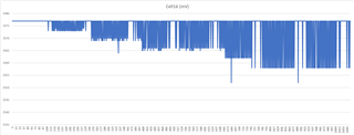
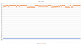
I am using BQ76952 in 16S configurations on the LFP battery Pack. Facing fluctuations on 16th number cell voltage measurement around 15mV on steady state and other cell voltage around 1mV which is normal. Below are the Firmware config and Images details.
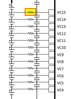
-> All Cell image and check 16th yellow cell.
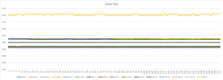
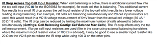
-> Below is 1st cell vs 16th cell
Can you please let me know what can be the cause of this.
// Configures all parameters in device RAM
// Enter CONFIGUPDATE mode (Subcommand 0x0090) - It is required to be in CONFIG_UPDATE mode to program the device RAM settings
// See TRM for full description of CONFIG_UPDATE mode
CommandSubcommands(SET_CFGUPDATE);
// After entering CONFIG_UPDATE mode, RAM registers can be programmed. When programming RAM, checksum and length must also be
// programmed for the change to take effect. All of the RAM registers are described in detail in the BQ769x2 TRM.
// An easier way to find the descriptions is in the BQStudio Data Memory screen. When you move the mouse over the register name,
// a full description of the register and the bits will pop up on the screen.
// 'Power Config' - 0x9234 = 0x2D80 //9E0
// Setting the DSLP_LDO bit allows the LDOs to remain active when the device goes into Deep Sleep mode
// Set wake speed bits to 00 for best performance
BQ769x2_SetRegister(PowerConfig, 0x27A8, 2); //Power Config
// 'REG0 Config' - set REG0_EN bit to enable pre-regulator
//BQ769x2_SetRegister(REG0Config, 0x01, 1); // doubt
// 'REG12 Config' - Enable REG1 with 3.0V output (0x0B for 3.0V, 0x0F for 5V)
BQ769x2_SetRegister(REG12Config, 0x0B, 1);
BQ769x2_SetRegister(REG12Config, 0x0F, 1);
// Set CFETOFF pin to Config (AFE_CS to oin enable)
BQ769x2_SetRegister(CFETOFFPinConfig, 0x4A, 1);
// Set DFETOFF pin to measure Cell Temperature - 0x92FB = 0x87 (set to 0x00 to disable) // set TS4 to measure cell temperature
BQ769x2_SetRegister(DFETOFFPinConfig, 0x07, 1);
// Set up ALERT Pin - 0x92FC = 0x2A // 0x22
// This configures the ALERT pin to drive high (REG1 voltage) when enabled.
// The ALERT pin can be used as an interrupt to the MCU when a protection has triggered or new measurements are available
// The Alert pin to measure Data ready
BQ769x2_SetRegister(ALERTPinConfig, 0x22, 1);
// DA Configuration.
BQ769x2_SetRegister(DaConfiguration, 0x06, 1); //Set Centiamp (10 mA) units are selected for user-amps.
// Current Calibiration CC Gain.
BQ769x2_SetRegister_f(CCGain, CC_GainValue, 4);
// Current Calibiration Capacity Gain.
Capacity_GainValue = CC_GainValue * 298261.6178;
BQ769x2_SetRegister_f(CapacityGain, Capacity_GainValue, 4);
Subcommands(CCGain, 0x00, R);
Subcommands(CapacityGain, 0x00, R);
// Set TS1 to measure Cell Temperature - 0x92FD = 0x87 //0x87
BQ769x2_SetRegister(TS1Config, 0x07, 1);
// Set TS2 to measure Cell Temperature - 0x92FE = 0x87
BQ769x2_SetRegister(TS2Config, 0x07, 1);
// Set TS3 to measure Cell Temperature - 0x92FF = 0x87
BQ769x2_SetRegister(TS3Config, 0x07, 1);
// Set HDQ to measure Master Otuput Slave Input - 0x9300 = 0x00
//BQ769x2_SetRegister(HDQPinConfig, 0x00, 1); // No thermistor installed on EVM HDQ pin, so set to 0x00
// Set DDSG TO measure short circuit detection
BQ769x2_SetRegister(DDSGPinConfig, 0xA2, 1);
// 'VCell Mode' - Enable 16 cells - 0x9304 = 0xFFFF; Writing 0xFFFF sets the 16 cells
BQ769x2_SetRegister(VCellMode, 0xFFFF, 2);
// Set up Protection Configuration Register Field Descriptions Disable all
BQ769x2_SetRegister(ProtectionConfiguration, 0x0000, 2);
// Enable protections in 'Enabled Protections A' 0x9261 = 0xBC
// Enables SCD (short-circuit), OCD1 (over-current in discharge), OCC (over-current in charge),
// COV (over-voltage), CUV (under-voltage)
BQ769x2_SetRegister(EnabledProtectionsA, 0x80, 1);
// Enable all protections in 'Enabled Protections B' 0x9262 = 0xF7
// Enables OTF (over-temperature FET), OTINT (internal over-temperature), OTD (over-temperature in discharge),
// OTC (over-temperature in charge), UTINT (internal under-temperature), UTD (under-temperature in discharge), UTC (under-temperature in charge)
BQ769x2_SetRegister(EnabledProtectionsB, 0x00, 1);
// Enable protections in 'Enabled Protections C' 0x9263 = 0x4F
BQ769x2_SetRegister(EnabledProtectionsC, 0x41, 1);
// 'Default Alarm Mask' - 0x..82 Enables the FullScan and ADScan bits, default value = 0xF800
BQ769x2_SetRegister(DefaultAlarmMask, 0xF882, 2);
// Set up Cell Balancing Configuration - 0x9335 = 0x0B - Automated balancing while in Relax or Charge modes
// Also see "Cell Balancing with BQ769x2 Battery Monitors" document on ti.com
BQ769x2_SetRegister(BalancingConfiguration, 0x03, 1);
BQ769x2_SetRegister(CellBalanceInterval, 0x02, 1); //Cell Balance Interval 5 Seconds
BQ769x2_SetRegister(CellBalanceMaxCells, 0x06, 1); //Cell Balance Max Cells 5 Cells
BQ769x2_SetRegister(CellBalanceMinCellVCharge, CombineConfigPacket.BMSDetailsConfiguration.BalanceStartVoltage, 2); //Cell Balance Min Cell V (Charge) 3100mV
BQ769x2_SetRegister(CellBalanceMinDeltaCharge, CombineConfigPacket.BMSDetailsConfiguration.BalanceWindow, 1); //Cell Balance Min Delta (Charge) 30mV
BQ769x2_SetRegister(CellBalanceStopDeltaCharge, (CombineConfigPacket.BMSDetailsConfiguration.BalanceWindow - 10), 1); //Cell Balance Stop Delta (Charge) 20mV
BQ769x2_SetRegister(CellBalanceMinCellVRelax, CombineConfigPacket.BMSDetailsConfiguration.BalanceStartVoltage, 2); //Cell Balance Min Cell V (Relax) 3200mV
BQ769x2_SetRegister(CellBalanceMinDeltaRelax, CombineConfigPacket.BMSDetailsConfiguration.BalanceWindow, 1); //Cell Balance Min Delta (Relax) 30mV
BQ769x2_SetRegister(CellBalanceStopDeltaRelax, (CombineConfigPacket.BMSDetailsConfiguration.BalanceWindow - 10), 1); //Cell Balance Stop Delta (Relax) 15mV
// Set up CUV (under-voltage) Threshold - 0x9275 = 0x31 (2479 mV)
// CUV Threshold is this value multiplied by 50.6mV
BQ769x2_SetRegister(CUVThreshold, 0x31, 1);
// Set up COV (over-voltage) Threshold - 0x9278 = 0x55 (4301 mV)
// COV Threshold is this value multiplied by 50.6mV
BQ769x2_SetRegister(COVThreshold, 0x55, 1);
// Set up OCC (over-current in charge) Threshold - 0x9280 = 0x05 (10 mV = 10A across 1mOhm sense resistor) Units in 2mV
BQ769x2_SetRegister(OCCThreshold, 0x05, 1);
// Set up OCD1 Threshold - 0x9282 = 0x0A (20 mV = 20A across 1mOhm sense resistor) units of 2mV
BQ769x2_SetRegister(OCD1Threshold, 0x0A, 1);
// Set up SCD Threshold - 0x9286 = 0x05 (100 mV = 100A across 1mOhm sense resistor) 0x05=100mV // 0x02=40 mV(31mV)
BQ769x2_SetRegister(SCDThreshold, 0x06, 1);
// Set up SCD Delay - 0x9287 = 0x03 (30 us) Enabled with a delay of (value - 1) * 15 µs; min value of 1
BQ769x2_SetRegister(SCDDelay, 0x02, 1);
// Set up SCDL Latch Limit to 1 to set SCD recovery only with load removal 0x9295 = 0x01
// If this is not set, then SCD will recover based on time (SCD Recovery Time parameter).
BQ769x2_SetRegister(SCDLLatchLimit, 0x01, 1);
// Exit CONFIGUPDATE mode - Subcommand 0x0092
CommandSubcommands(EXIT_CFGUPDATE);