This thread has been locked.

If you have a related question, please click the "Ask a related question" button in the top right corner. The newly created question will be automatically linked to this question.

LM5034: Max duty fixing points

Part Number: LM5034

Tool/software:

Hi Team...

I have designed an isolated DC-DC converter with the followings specifications.

Input voltage range : 12-36V typical 28V

Output : 250W (Voltage 50V & Current 5A)

Step-up transformer turns ratio: 1:5

considered switching frequency: 500KHz

Design considered Efficiency : 91%

As of my design consideration I have selected LM5034 for wide range input support, maximum duty 80% configuration and interleaved section each can source 125W output category.

But now I am facing duty cycle limitation issue from the controller.

I have verified the Duty cycle will be limited based on UV lockout, Current sense and compensation input in datasheet.

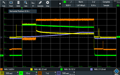
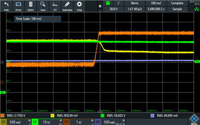
My issue is while load the output in single section around 0.5A load output 50V getting dipped upto 46V in 12V input and 28V input also.

As of my analysis I have done few debugging methods to find out the actual duty limiting scenario.

1) Bypassed the current limiting option to identify the duty limiting happened due to current sense option - But no improvement issue remains same.

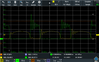
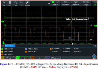
2) Probed the compensation loop response and controller COMP1 pin with respect to output voltage dip and switch node - Found compensation sourcing the feed back to adjust the max duty but controller still maintain the same duty.

I wanted to know why its behave like that is that controller issue, transformer gain transfer issue or any other further verification I have to done or what.... Please explain experts...

  • I have forgot to mention one more point as of my calculation with 12V input controller can be generated maximum duty, Because UV lock out is fixed after crossing 12V (1.25V threshold for max duty)

  • Hi Prasanna,

    The gain seems to be very close to the limit. 12*5*0.8 = 48V.

    • What is the maximum duty cycle do you observe on oscilloscope? Can you share a waveform along with V_COMP1 along with VIN, IOUT test conditions (12VIN, 28VIN)? Measure V_COMP1 on one side of 10k ohm resistor with the other side connected to COMP1 pin to avoid probing effect.
    • What happens to the output voltage, if the load current further increases?
    • What is RDCL value with respect to RT? Did you leave COMP1 (COMP2) open?

    Please note that during the year end, our team runs lean, expect some delays.

    Regards

    Hemanth

  • Hello Hemanth,

    1) (a) Please find the observed maximum duty probed image in below link (As per captured maximum duty is 72%)

    /cfs-file/__key/communityserver-discussions-components-files/196/Duty-calculation.pdf

    (b) Please find the Compensation output-CH1 (Yellow - input to the opto coupler), Vout-CH2 (green), Vcomp-CH3 (Orange) and Iout-CH4 (Purple)

                         Image 1 overall capture                Image 2 During load current increase output voltage getting dip showed in 100ms

    (c) Below mentioned image captured in output switch node response while loading the output in 28V input

    CH1 (Yellow) - SEC-Series FET drain, CH2 (Green) - SEC-shunt FET drain, CH3 (Orange) - Vout, CH4 (Purple) - Input current

                    Image 3 Vout at 0.5A load

    2) During output load increase output voltage also getting decreases shown in image 1load varied from 166mA to 500mA.

    3) (a) As per datasheet recommendation 16.5Kohms resistor is used in RDCL & RT to fix the 500KHz switching frequency and max duty.

    (b) No Comp 1 & 2 pins are connected to compensation network through 2-CH opto coupler  (MOCD207M).

    Please revert back if any further clarification required in shared data.

    Regards

    Prasanna S

  • Hello Prasanna,

    Please expect a delay in response due to the holidays.

    Regards,

    Jonathan Wong

  • Hi,

    Please provide your schematics for review.

  • Hello Jonathan,

    No issues, I understand the situation. Meanwhile I proceeded my other section validation.

    Regards,

    Prasanna

  • Prasanna,

    Beyond this point, this issue is taken over by Mr Hong. He requested for schematic for his review. Can you share schematic?

    Regards
    Hemanth

  • Dear Mr. Hong & Hemanth,

    As per our organization internal process schematic should not share to any external communication, Queries and clarification related. So I am preparing draft SCH for better understanding, once completed draft will be shared.

    Possibly it will be done by end of today.

    Regards

    Prasanna

  • Hello Hong,

    Please find the enclosed draft SCH for better understanding the circuit.

    Draft SCH for the forward converter

    Kindly Revert back if any clarity required.

    Regards,

    Prasanna

  • Hi,

    My review to this shows the max duty cycle you got is 72%, right?

  • Hi Hong,

    Happy new year..!!!

    Based on resistor used in RT, DCL pin and as per datasheet you are saying the 72% max duty, Right..?

    But as of observed and my boost calculation the max duty is not observed.

    And my query is where the duty is getting limited and why the output voltage getting dip based on load increase.

    Regards,

    Prasanna

  • Hi,

    The max duty cycle typically can be obtained is 76% at UVLO = 1.3V, close to  but < 80% at UVLO = 1.25V typically. 

    So 72% is reasonably taken as max can be obtained on this particular unit, that is, this particular unit duty cycle cannot be further bigger as it is already within the datasheet limitation.

  • Hi Hong,

    as your calculation 72% duty is not observed in controller output, I have verified in both channels issue remains same.

    Still no clear clarity, Output Voltage getting reduced due to transformer gain or not and what are the possibilities to limit the duty even voltage reduce also....

    Please explain...

    Regards

    Prasanna

  • Hi,

    This device max duty cycle individually may not be 80%, and 70% is possible. So you need to design transformer turns ratios to leave enough margin to allow max duty cycle of its minimum value at about 70%.

    Your waveform shows 72% duty cycle which is likely the max duty cycle for that individual device. 

    If you see max duty cycle is different at different operation, please provide each operation condition, max duty cycle, and associated waveforms. Please measure the duty cycle at the IC pins. 

  • Hi Hong,

    Please find the duty cycle variation based on feedback compensation adjustment analysis document attachment.

    As of the validation we understood the duty is not getting varied and its been limited by the controller.

    Kindly refer the document and conclude which case this duty getting limited.

    LM5034 Max duty query.pdf

    Prasanna S

  • Hi,

    What is the below waveform? Is the duty cycle actually t1/T?

  • Hi Hong,

    It was mentioned below the waveform probed image, Since the active clamp MOSFET as operating inverting operation OFF time the gate will be MOSFET ON time.

    Prasanna

  • Hi,

    To help understand your waveforms, please provide the waveforms at LM5034 pins.

  • Hello hong,

    Shared waveform is probed in LM5034 IC's Pin no. 12 (AC2) since it is an active clamp gate drive you have to consider the OFF time duty to drive the P-CH gate.

    The active clamp MOSFET (AC2) gate will be inverse to the Main MOSFET (OUT2) gate.

    Hope this clears your doubt...

    Regards

    Prasanna S

  • Hi,

    The specified duty cycle means OUT pin duty cycle. Please show OUT pin duty cycle or indicate which waveform is for OUT pin waveform to show duty cycle you measured. The external circuit like inverse can affect the duty cycle so not able to judge the LM5034.

  • Hello hong,

    I have verified the duty is not getting changed in switching MOSFET OUT1 & OUT2 pins also. instead of verifying waveforms try to suggest the possibilities or cases to operate the converter in fixed duty.

    We have verified in all possibilities like I said from the begin Input voltage varied from 12V to 36V, Feedback (comp pin) input varied as per the opto coupler sourcing current. At last we planned to replace the converter with new one.

    If in that case also the duty is not varied what will be causes to operate the controller in fixed duty.

    That is my query... Try to find out the solution. I won't raise query without verifying such cases.

  • Hi,

    Please provide OUT pin waveforms to help understand. Why do you not want to provide OUT pin waveforms?

  • Hi,

    The duty cycle is also affected by CS pin since this is a current mode control. Please also provide CS and COMP along with OUT waveforms. These together can help to provide some clues.