This thread has been locked.

If you have a related question, please click the "Ask a related question" button in the top right corner. The newly created question will be automatically linked to this question.

TPS65987DDK: 5V is not being supplied to VBUS.

Part Number: TPS65987DDK
Other Parts Discussed in Thread: TPS65987

Tool/software:

Hi team,

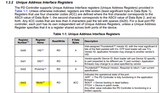
Supplying 5V to the PP_HV of the TPS65987 and also supplying +3.3V separately.

Although the patch has been successfully written from the CPU to the PD, occasionally +5V is not supplied to the VBUS side.

This issue is resolved by powering down the device, restarting it, and rewriting the patch.

What could be the possible causes of this issue?

Best regards,

Kyohei

  • Hi Kyohei,

    There is not enough information to debug your issue, can you answer the following questions?

    How is the device booting? Dead battery or internally powered?

    How are you confirming the patch is successfully being written?

    Do you have a PD log you can share of the connection? A PD log is a capture of the CC communication between Type-C PD port partners.

    What is being connected on the far-end? Is it a power sink only device?

    Please share the pjt you are using, and specify which version of the GUI you are using.

    When it fails (no-5V) can you read the status (0x1A) register and report what you read? And do the same for the working case.

    Thanks and Regards,

    Chris

  • Hi Chris,

    Thank you for your reply.

    I have confirmed with the customer, so I am sharing it with you.

    ≫1. How is the device booting? Dead battery or internally powered?

    We are restarting the device by turning the AC power of the equipment off and on again.

    ≫2. How are you confirming the patch is successfully being written?

    We determine this by reading the “Command Execution Successful?” register after executing commands (such as PTCs).

    ≫3. Do you have a PD log you can share of the connection? A PD log is a capture of the CC communication between Type-C PD port partners.

    ≫4. What is being connected on the far-end? Is it a power sink only device?

    ≫5. Please share the pjt you are using, and specify which version of the GUI you are using.

    I have summarized it in Excel and will send it via private message. In addition, I will also send the circuit diagram and the project used for writing.Please approve the FRIENDSHIP request.

    ≫6. When it fails (no-5V) can you read the status (0x1A) register and report what you read? And do the same for the working case.

            Work         Not Work

      [ 8] : 0x00        0x00

      [ 7] : 0x00        0x00

      [ 6] : 0x00        0x00

      [ 5] : 0x00        0x00


      [ 4] : 0x00        0x42

      [ 3] : 0x20        0x00

      [ 2] : 0x00        0x00

      [ 1] : 0x7F        0x7F

    Please confirm the above.

    Best regards,

    Kyohei

  • Hi Kyohei,

    ≫1. How is the device booting? Dead battery or internally powered?

    We are restarting the device by turning the AC power of the equipment off and on again

    Ok, this should be fine

    ≫2. How are you confirming the patch is successfully being written?

    We determine this by reading the “Command Execution Successful?” register after executing commands (such as PTCs).

    If you read the mode register, does it read APP after patching is complete?

    If, during the failing case, you do not read APP, it could be an issue with patch loading.

    ≫3. Do you have a PD log you can share of the connection? A PD log is a capture of the CC communication between Type-C PD port partners.

    ≫4. What is being connected on the far-end? Is it a power sink only device?

    ≫5. Please share the pjt you are using, and specify which version of the GUI you are using.

    I have summarized it in Excel and will send it via private message. In addition, I will also send the circuit diagram and the project used for writing.Please approve the FRIENDSHIP request.

    I did not see your request, but sent a request to you. Will wait for this info.

    Thanks for the register log, it appears like your device is acting as legacy, but that should not prevent 5-V from showing up. I'll wait to see the excel sheet before providing more feedback.

    The .pjt file might help here.

    Thanks and Regards,

    Chris

  • Hi Chris,

    Thank you for your reply.

    I have sent the PD log, the project for writing, and the connection circuit diagram via private message.

    Please check them.

    Best regards,

    Kyohei

  • Hi Kyohei, 

    Chris is currently out of office this week. Please expect some delay in responses. 

    Thank you in advance!

    Best Regards, 

    Aya Khedr 

  • Hi Aya,

    Thank you for your reply.

    I'll wait for Chris a little .

    Best regards,

    Kyohei

  • Hi Kyohei, 

    Thank you!

    Best Regards, 

    Aya Khedr

  • Hi Aya,

    Do you know how long Chris will be on leave? If it will take more time, I am thinking of asking the question in a new thread.

    Best regards,

    Kyohei

  • Hi Kyohei, 

    Thank you for your patience. Chris will be back this week. 

    Best Regards, 

    Aya Khedr

  • Hi Aya,

    OK. Thank you!

    Kyohei

  • Hi Kyohei,

    Can you confirm that the mode register reads "APP" in both failing and non-failing cases? During the failing case, would it be possible to obtain an I2C log of the flash process? Also the same for a working case to compare them?

    Can you share the PD analyzer files in the future? They are a little easier to work with than an excel. From the logs, there is not anything obvious preventing 5-V sourcing.

    Is there any differences in execution between the working and non-working case? If I understand, all you are doing is powering the system up, loading the fw image, and connecting a device to the port to do 5-V source? Does the connection to the type-c port always happen after power up, or is the port always connected? And what is being attached to the port? Is it a sink only device?

    Thanks and Regards,

    Chris

  • Hi Chris,

    >Can you confirm that the mode register reads "APP" in both failing and non-failing cases? During the failing case, would it be possible to obtain an I2C log of the flash process? Also the same for a working case to compare them?

    Is the mode register the 0x5D register in the Technical Reference Manual?

    Is it correct to understand that it refers to the FPGA-PD patch?

    >Can you share the PD analyzer files in the future? They are a little easier to work with than an excel. From the logs, there is not anything obvious preventing 5-V sourcing.

    The PD analyzer file is only available at startup. If the 5V output is not present and the system does not start, nothing will be displayed on the analyzer. The last ‘Power ON’ in the Excel file indicates that the 5V output is not present.

    >Is there any differences in execution between the working and non-working case? If I understand, all you are doing is powering the system up, loading the fw image, and connecting a device to the port to do 5-V source? Does the connection to the type-c port always happen after power up, or is the port always connected? And what is being attached to the port? Is it a sink only device?

    The system startup (source side) involves loading the PD patch with FW, supplying 5V from the source side, and then starting the sink side. At this time, the USB cable between the source and sink is connected before startup. The sink side starts with a sink-specific ROM.

    Best regard,

    Kyohei

  • Hi Kyohei,

    Is the mode register the 0x5D register in the Technical Reference Manual?

    No, it should be register 0x03 in the TRM.

    This is the operational mode of the PD controller.

    From the log you shared, (8) does not even negotiate PD, so it may be an issue with the patch loading the 8th time. Provided the initial voltages are the same (PD power, 5V PPHV power, etc.) are all up in time, it seems like the PD controller is not negotiating. We see some noise(?) or toggling on the CC lines(orange), but do not see it settle at ~1.7-V like in the working cases. This indicates a failure of connection.

    The PD analyzer file is only available at startup. If the 5V output is not present and the system does not start, nothing will be displayed on the analyzer. The last ‘Power ON’ in the Excel file indicates that the 5V output is not present.

    Oh, I just meant the raw PD analyzer files (.tdc) instead of the .csv. I should have the tool to read it directly. Either format is fine, but using the .tdc is a bit easier.

    The system startup (source side) involves loading the PD patch with FW, supplying 5V from the source side, and then starting the sink side. At this time, the USB cable between the source and sink is connected before startup. The sink side starts with a sink-specific ROM.

    Sounds good. When it works and when it fails, can you report the mode register?

    Thanks and Regards,

    Chris