This thread has been locked.

If you have a related question, please click the "Ask a related question" button in the top right corner. The newly created question will be automatically linked to this question.

LM5149: Output of LM5149 drops out of regulation at very low load currents

Part Number: LM5149
Other Parts Discussed in Thread: LM70860, LM70660, LM5148, CSD19532KTT, CSD19532Q5B

Tool/software:

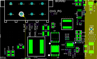
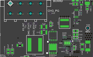
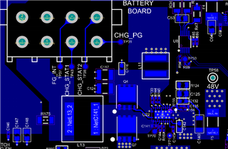
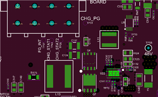
I am currently debugging a LM5149 design for a high power industrial application. I am trying to troubleshoot an issue with the output voltage dropping out of regulation at lower than expected output currents. We expect to achieve 4A, when the output drops by several volts at around 1A of output current. As I debug the issue, I would like to force the regulator to run in continuous switching mode to compare the performance. However, when I ground pin 18 as noted in the datasheet, the regulator instead outputs zero volts, and probing the SW node reveals that the regulator is not switching at all. I have verified that the enable pin is still being pulled up to the input voltage. What could be causing this?

  • Hi Taylor,

    Send on the schematic and a completed quickstart file for this. The likelihood is you're getting noise on the current sense, causing current limit too early. Is there any RC filter on the current sense pins?

    We may need to review the layout as well.

    Regards,

    Tim

  • Thanks for the response Timothy, hope you enjoyed a good holiday season.
    This problem is a finicky one. I'll provide some more context. I'll attach the WEBENCH reference schematic that was used. If layout and schematic files are needed, let me know and I will work to get an NDA in place with our client. 
    We are using the LM5149 to create a 15V rail from 50V plus or minus a few volts. We have a rev 1 board design that functions as expected, however the ferrite core inductor was heating up beyond our comfort level, so a composite core inductor with lower DCR was chosen as its replacement. In the second spin, a few parts that were deemed insignificant were moved to the bottom layer to save pick and place space, namely the switching frequency select resistor and the configuration set resistor etc. Other than those changes, layout changes to the second spin of the board were absolutely minimal, with no changes in the voltage or current feedback traces, and no changes in the high current loop section. However, the second revision of the board is having the above-mentioned issue where the output voltage drops out of regulation at around 1A of DC load current. I will not go into the trouble I had with setting the controller to continuous switching mode which I mentioned in the post, however I am curious if these issues are related, as with the revision 1 design I was able to set it to switch continuously without issues.
    As I have worked on debugging this issue, I have worked in both directions: Starting at the rev 2 design and making mods to work back to the rev 1 design until hopefully something fixed the problem, and conversely starting at the rev 1 design and making mods to work forward to the rev 2 design until something broke. I was not able to succeed with either of those strategies. 
    I have collected many oscilloscope screenshots showing the external FET gate signals, inductor current, and SW node. Node labels are on the right hand side of the screen. I also gathered some measurements of the current sense voltage lines with a differential probe. This is when I noticed the fundamental difference between the two revisions. As load current increases, the first design revision first increases switching frequency to keep up with the load and keeps the peak inductor current capped, but then after a certain point allows the inductor current to rise past that to accommodate higher load currents. The second design revision fails at the second step. It will not allow the peak inductor current to rise above what looks to be about a 2.5A threshold (~23mV of current sense voltage) even when the output voltage sags out of regulation. According to the datasheet this level is around when the Active EMI filtering activates. Could this be playing a role?
    I agree that the only thing that seems to make sense is that the converter is cycle per cycle current limiting, but according to my measurements this is happening much too soon. Looking at the attached screenshots, the rev1 design allows the current sense voltage to increase much more than the rev2 design. It seems like the IC is shutting the cycle down quite early. And since the two designs are almost identical in layout, I can't see why one would have more noise on these lines than the other. I implemented a low pass filter to test this theory as you said, which did not exist before. I used two 10 Ohm resistors with a differential 0.01uF capacitor right at the IC pins. This had no effect on the rev 2 designs performance.
    I am running out of things to try, which brings me here. Do you have any recommendations for further debugging? I think at this point feedback on the layout is of value. Are these parts particularly sensitive to ESD or heat?
    Here's a link to some debug files, including the Webench output and a number of scope plots comparing my original design with my new one: www.dropbox.com/.../AMAc6DOz3f8UKi6Cr06kOtg
  • Hi Taylor,

    Sorry for the late reply given the Xmas break. I'm not able to access dropbox unfortunately. Please attach the files here, particularly a completed quickstart calculator file.

    Regards,

    Tim

  • Tim, thanks for the reply, I've attached the Webench output to this post. I've also attached the PDF of my waveforms. 

    LM5149_3.pdf15V buck debugging.pdf

  • Thanks, Taylor. Send on the completed quickstart file - that's the key to determining losses, stability, etc. Also send the layout (screenshots are fine).

    https://www.ti.com/tool/LM5148-LM25148DESIGN-CALC

    --

    Tim

  • Hi Taylor,

    Just looking at the quickstart, you could do 6A with a converter (integrated FETs), e.g. LM70860 80V/6A, LM70660 65V/6A, and get smaller solution size and much easier implementation.

    The 9mΩ shunt (current sense resistor) only gives a current limit of 5.8A, whereas typical is 120-150% of full load, e.g. 8-9A.

    More important, I see the high-side FET is an old gen 100V Infineon device, BSC265N10LSFGATMA1. WEBENCH should have recommended an 80V FET here, same rating as the controller. No need for 100V and compromise efficiency.

    But here is the real issue - the low-side FET, CSD19532KTT, is not a logic-level gate drive device, which is defined by Rdson rated at Vgs = 4.5V. The FET is not suitable for a 5V gate driver, hence why it didn't work in FPWM. You can see from the curve below that the Miller plateau voltage is right around 5V, so there is no gate overdrive with a 5V gate drive amplitude. Also, this D2PAK package is huge, has high inductive parasitics, and is unsuitable for this low-current application (note its Qrr is 326nC, making it super lossy). Take a look at the FETs used in the LM5149 EVM and what's referenced in the LM5148/9 data sheet.

    Regards,

    Tim

  • Hi Timothy,
    I tried testing with 3 new low side mosfets. Unfortunately, none of them worked. I tried testing with
    1. IAUC50N08S5L096ATMA1 (datasheet recommended part),
    2. BSC034N10LS5ATMA1,
    3. FDMS007N08LC.
    I attached a PDF of my testing results. This was the only part I changed when doing our testing. Is there anything else that stands out to you that you think we should look into? Or any other criteria we missed when selecting an alternative mosfet? We are using XGL1010-153 as our switching inductor. We were using MSS1210-153MEB on the rev 1 board. The changes between these two inductors are minimal, but I just wanted to let you know incase we are missing something.
    I did have a question regarding the Active EMI Filter. To disable the AEF, do we need to connect the CNFG pin (3) directly to ground after startup? Or is having a 40.2K ohm resistor to ground disable this feature?
    If the AEF is active but we aren’t supplying any voltage to the AEFVDDA pin (22), could this cause any problems to the IC? We currently only have a ceramic capacitor (.1uF) to ground on that pin. This could be totally unrelated to our problem, but I just wanted to verify.
    • IAUC50N08S5L096ATMA1
      • This is the recommended part on the LM5149 datasheet.
      • This had the worst response out of all the mosfets.
    • BSC034N10LS5ATMA1
      • This had a worse response than the original CSD19532Q5B part.
    • FDMS007N08LC
      • This had a similar behavior to the current part in the schematic (CSD19532Q5B).

    Low-Side Mosfet Testing.pdf

  • Hi Taylor,\

    These FETs seems fine, as they are logic-level devices suitable for 5V gate drive.

    You may have noise on the current sense lines. Are you in contact with a TI FAE? It would be good to setup a meeting to review your design.

    My understanding is you can leave all the AEF pins open circuit.

    Regards,

    Tim

  • Tim, Thanks for the continued support. We are not currently in touch with an FAE. Could you  help us get in contact with someone? 

  • Where are you located and what company?

  • Hi Timothy, I am a colleague of Taylor's and we are working on this problem together. We work at Indesign and are located in Indianapolis, Indiana. 

  • Let me check on this and get back to you on Monday.

  • Hi Timothy, did you have any updates on if you could connect us to someone? 

  • Hi Arya,

    Apologies for the belated reply as yesterday was a holiday. Let me check now and see if I can get a contact for you.

    Regards,

    Tim

  • Hi Tim, just checking back in here to see if you have any update on a contact. Thanks!

  • No luck yet with that. But I was just looking at your files again. The rev 2 design looks a lot more stable, but you mention the duty cycle is getting clamped. This could be the peak current limit engaging.The quickstart file shows 9mΩ for the current sense resistor, which implies 60mV/9mΩ = 6.6A peak current limit. Your waveforms show 2.5A peak current. Is the resistance actually 9mΩ? Even this is low for a 6A load – it should be more like 6mΩ. Also check the voltage at the ISNS+ and VOUT pins at the IC. Add an RC filter if there is high-frequency noise near the peak. How are the current sense lines routed back to the IC - is there a GND plane between the traces and the power stage components, or is noise being picked up from the inductor or the gate drive traces?

    Regards,

    Tim