This thread has been locked.
If you have a related question, please click the "Ask a related question" button in the top right corner. The newly created question will be automatically linked to this question.
Tool/software:
Hello,
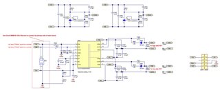
I am trying to design the schematic of UCC21530. While examining application notes and reference designs, I noticed some differences.
In the picture I atteched, there are 2 ports named "Coma" and "Comb".
Hello,
Thank you for you question. Our team is out of office on Dec 24 and Dec 25 due to US holiday. Please also expect delay in our response during the holiday season period (from Dec 24 through Jan 2).
Thank you for your patience,
Leslie
Hi Nafi,
In this schematic example, they are using a negative voltage bias on VSSA/VSSB. Because of this, they are naming the source connection to the load MOSFETs "COM" (COMA for channel A and COMB for channel B). This is not a necessary application as a negative voltage bias is not always necessary.
In common applications, VSSA and VSSB would be connected to the source of the load MOSFETs respectively.
Here is an example reference design: https://www.ti.com/tool/TIDA-00366
Regards,
Hiroki