This thread has been locked.

If you have a related question, please click the "Ask a related question" button in the top right corner. The newly created question will be automatically linked to this question.

TPS61023EVM-052: TPS61099EVM-023

Part Number: TPS61023EVM-052
Other Parts Discussed in Thread: TPS61099EVM-023

Tool/software:

Hello Travis,

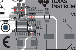
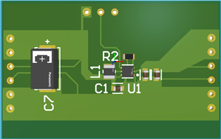
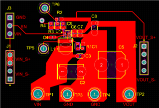
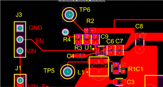
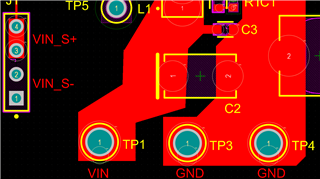
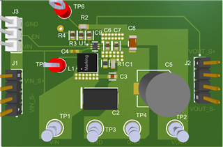
As you mentioned, I have made the adjustments. Since I use a MacBook Air M1, I cannot use Altium; instead, I am using the EasyEDA Pro Desktop software. I researched and implemented the adjustments as per your suggestions. I cannot thank you enough for your support.

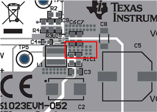
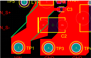
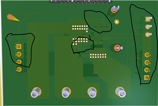
and one note ı draw it later -052 when you accept this desing.

  • Hi Muhammet,

    No need to thank me again. First, please place component in the same way as the EVM did. Otherwise, it'll be harder to route wires correctly without proper  component placement.

    I'm not sure how to operate Easy EDA. But I think after placing polygon pour, the next step will be assigning nets for these polygon. As you can see the polygon is not connected to your components pins. This is because these polygon is not assigned with the same net with the component pins

    And then, use polygon pour on bottom layer and pour the entire bottom layer with GND. Place vias near the GND pad of C2 and C3.

    Best Regards,

    Travis

  • Dear Travis,

    I have updated one of the PCB designs TPS61099EVM-023. I would appreciate it if you could review and verify the changes at your earliest convenience.

    Thank you for your support.

    Best regards,

  • Hi Muhammet,

    Your layout is good. This application note describes the design considerations about boost layout. You can look at this note to understand why the PCB placement should be like this.

    TPS61022 and TPS61023 Boost Converters Layout Guidelines

    Best Regards,

    Travis

  • Hi Travis,
    I hope you are doing well. You have been incredibly helpful throughout this process, and I am truly grateful. I want to extend my heartfelt thanks for all your support. By the way, I have also completed the EVM-052 design. Do you see any errors in the PCB layout?

  • Hi Muhammet,

    The layout is fine for top layer. Please pour bottom with GND and place vias on GND polygon near Cout.

    Also, please use +-45 degree and +-90 degree on polygon outline. This does not affect PCB function, but it's standard principle to ensure maximum usage of space.

    Best Regards,

    Travis

  • Hi Travis,
    I have made the adjustments you mentioned. This was my first PCB design project in my life, and thanks to you, I learned what to do and how to do it. I can't thank you enough for that. I am truly grateful to you.