This thread has been locked.

If you have a related question, please click the "Ask a related question" button in the top right corner. The newly created question will be automatically linked to this question.

TPS40322 design example question

Other Parts Discussed in Thread: TPS40322

hi there,

I have a few questions for the design example (Figure 23) in http://www.ti.com/lit/ds/symlink/tps40322.pdf.


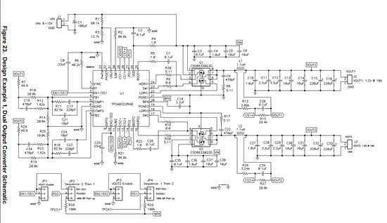
  1. What's the purpose of these 1 ohm resistors?  R4=1ohm between VDD and VIN.  R5=1.0R & R22=1.0R at the BOOTx pins.

thanks,
Titus 

  • I guess R4 & C2 work as a delay circuit?

  • Titus,

    These resistors serve different purposes.

    R4 is a small filter for the bias voltage for the IC. Typically the Vin is quite noisy because the high side FET draws power from it, and imposes a very high di/dt. This causes a fair amount of noise on Vin, and R4 / C2 are intended as a filter.

    R5 and R22 serve to slow down the turn ON of the high side FET while not affecting the speed of the turn OFF. The power for the HDRV signal comes from the bootstrap cap C7, and when there is a turn ON pulse for HDRV, some gate current must flow through R5. However, when the FET gets turned OFF, the gate current does not flow through R5. Normally it is desirable to limit the speed of turn ON of the high side FET, but the the turn OFF should be as fast as possible.

    Note that when the high side FET gets a gate pulse, when the absolute gate voltage (wrt ground) is still lower than BP6, some gate current will also come directly from BP6 and some from C7. So the initial speed of the gate charging is not affected much by R5.

    Conversely, R30 slows both the turn ON and turn OFF of the high side FET under all circumstances.

    MC.

  • Just curious if it is okay to do without the current sense CS+/- if i am certain my load won't be over the 10A limit?  How sensitive is it to the inductor and layout?  

  • Layout is very important with this device; just as it is with anycontroller.  The capacitor used in the current sensing circuit must be placed as close to the CS+ and CS- pins as possible, as stated in the data sheet.  Improper layout may result in start up issues. 

  • Also, I would never recommend that you "do without the current sense CS+/-" no matter how certain you may be regarding the output current regulation.  You should not leave the CS+/- pins open. The converter will have no short circuit protection without this signal.  You can set the threshold relatively high with the ILIM resistor if you feel it is limiting the converter within its normal operating conditions but a better layout an utilizing the built in protection features of the device would be best.

  • I don't know if it's okay to for me to ask a question under other's post, but if it isn't, please let me know then I'll create my own post to ask.

    I am also trying to understand the same power supply (TPS40322).

    Could you explain why the speed of turn ON of the high side FET should be slowed down, but the speed of OFF should be as fast as possible?

    And why the drain side of buffer (SW1) is connected to the output of the FET?

    Also wondering why there is a switch between BP9 and the pin 25 (BOOT1).


    Your reply would be appreciated.

    Thanks,


  • PW,


    1) As discussed in previous posts, the inductor current ramps up from some value X to another value Y during the ON time. Then during the OFF time it ramps back down from Y to X. The values of X and Y are determined by the system parameters Fsw, L, Vin, Vout and Iout. When the catch device is a FET, then X can actually be negative (such that current is in the direction from output, through the choke into the FETs). This will be the case any time when the load is less than (Y-X)/2. For example if Y = 4 and X = 2, then that implies that the load is 3A. But the delta of (Y-X) is not determined by the load, it is determined by Fsw, L, Vin, and Vout (but not Iout). In the same system, if the other parameters don’t change (Fsw, L, Vin, and Vout), then (Y-X) will always be 2A. If the load was 10A, then Y would = 11A and X would = 9A. If the load was 6A, then Y would = 7A and X would = 5A etc. So in this system, whenever the load drops below 1A (or (Y-X)/2), there will be a portion of the current that flows from choke to FETs. Whenever that happens, the most negative point of current is exactly when the catch FET turns OFF and the high side FET turns ON. Also, since current is flowing from choke to FETs at that point, this current will force the SW node to commutate high because it charges the parasitic capacitances at the SW node until the body diode of the high side FET starts conducting current back to Vin. For that case (when the load is less than (Y-X)/2) the speed of turn ON of the high side FET does not need to be reduced.


    However, most of the time for your average DC-DC switcher, the load is more than (Y-X)/2. So at the point when the high side FET turns ON, current is flowing from FETs to choke. In order to avoid shoot-through current, the controller will always turn the catch FET OFF first and then wait some dead time before turning ON the high side FET. During that dead time, the current must still flow, and it will flow in the body diode of the catch FET from ground to choke. This will continue until the high side FET turns ON, at which point the body diode must block any reverse current. When a body diode transitions from carrying current to reverse blocking, it is said to “recover”. Diode recovery is another discussion, but suffice to say that during recovery there is current flowing in the wrong direction in the diode, sometimes a very large amount of current, that is eventually snapped OFF very rapidly. This resulting extreme di/dt causes all sorts of problems including power dissipation in the body diode, and a lot of high frequency ringing in the parasitic elements attached to the cathode of the diode. The faster the imposed dV/dt on the diode, the more severe the recovery. So it is of benefit to turn the high side FET ON less rapidly so that the catch body diode has to deal with less recovery.


    The other side of the ON time is different. When the high side FET turns OFF, the only thing that happens is that the choke current (which is always from FET to choke at that point) will force the SW node to commutate low until the body diode of the catch FET conducts current from ground to choke. So there is no penalty to turning the high side FET OFF as rapidly as possible.


    2) The next questions is why is the low side of the HDRV buffer connected to SW node. This section of the controller is more a gate driver than a buffer, and this gate drive is referenced to the SW node rather than to ground or Vdd. That is, the whole driver circuit moves up and down with the SW node. This is because the high side FET drain is at Vin, and when the FET is ON, the source is also at Vin (through the RDS-ON), so in order to turn the FET ON properly, the gate must be above Vin. If the controller could only bring the gate as high as Vin, then the source would be at (Vin-(required gate voltage)), somewhere around 4 or 5 volts lower than Vin. That means that the Vds would also be around 4 or 5 volts, and the power dissipation in the high side FET would be prohibitive (and efficiency would be poor).


    In order to have a stable Vcc for the gate drive, the Vcc cap for the gate drive must also be referenced to the SW node. That is exactly the function of the BOOT cap (sometimes renamed to the BOOST cap). This BOOT(strap) cap is referenced to the SW node so that when the SW moves, this Vcc cap moves with it, thus providing a stable dedicated voltage source to power the flying high side gate drive circuit.


    So the whole HDRV circuit is flying, meaning that it moves with the SW node. The lower side of the gate drive (pin 23 SW1) is the reference for the high side gate drive and it is referenced to the source of the high side FET, because the drive for the high side FET must exist between gate and source.


    3) The next question is why there is a switch between BP6 and pin 25 (BOOT1).


    This switch is in parallel with the BOOT diode (not named in the diagram). The function of this diode is to charge, or more accurately replenish the charge on the BOOT cap when the SW node is low (when the catch FET is ON). The whole time that the SW node is high, the HDRV gate drive circuit is getting its power from the BOOT cap only and not from any DC source. So during that time, the BOOT cap discharges slightly as it provides power for the HDRV circuit. The only time its charge can get replenished is when the catch FET is ON, charged from BP6 through the BOOT diode.


    In a system where Vin is relatively low, anything less than 5V or so, the BOOT cap only would get charged to (Vin – dropout voltage of BP6 – BOOT diode drop). Sometimes this can be so low that there isn’t enough charge on the BOOT cap to properly turn the high side FET ON (depending on the high side FET device specs and the load operating point). So in order to extend the low end of Vin operation of the controller, there is an additional switch in parallel with the BOOT diode so that there is less drop when charging the BOOT cap when Vin is low.


    MC.

  • Thanks a lot for your thorough explanation, Martin!!  Now it makes much more sense to me!