This thread has been locked.

If you have a related question, please click the "Ask a related question" button in the top right corner. The newly created question will be automatically linked to this question.

UCC28070A: Do not operating

Part Number: UCC28070A
Other Parts Discussed in Thread: UCC28070, , UCC27518

Tool/software:

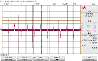
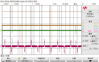
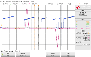
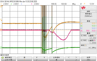
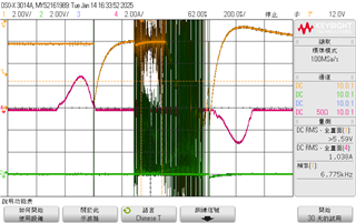
Hi teams, I want to ask why my boost pfc did not operate correct.

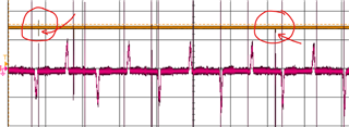
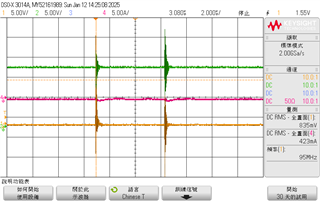
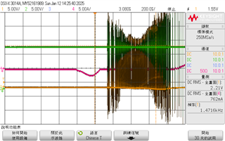
Below is my waveform , yellow one is MOSFET's Vgs and red one is input current.

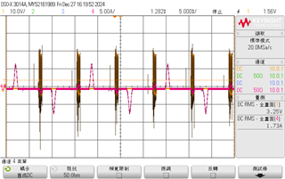
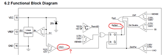
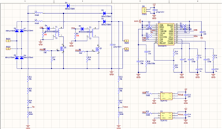
All components is followed by the excel that TI gave.

  • Hello, 

    The red current waveforms during the yellow Vgs switching indicates that PFC controller is attempting to operate, but stops suddenly for an unknown reason. 

    I suggest that the reason is that the UCC28070 controller or the gate-driver IC loses VCC bias power. Then restarts after VCC bias is restored each half-cycle. 
    Please check the VCC source to the PFC controller and/or gate-drive to ensure that it stays within specified limits continuously. 

    Regards,
    Ulrich

  • I ues DC power supply to give VCC(15V) source to PFC controller and gate-driver

  • Hello, 

    Please check the VCC voltage at the IC pins.  
    The DC source may have continuous output, but the voltage at the pins may be dropping out of spec.  

    If voltage stays in spec at the VCC + GND pins, then we have to look for another reason for the switching to stop. 
    Your yellow waveform is measuring Vgs of one of the MOSFETs.  
    Please measure GDA and GDB instead, to verify if the controller is stopping or if the gate-driver is stopping. 

    Regards,
    Ulrich

  • Okay, I'll test it tomorrow. If still have problems , I'll reply here.

    Thanks a lot Ulrich.

    Happy Holiday!

  • Hi Ulrich, I still got problems. Waveforms below, first one is the VCC voltage at the IC pin(yellow one), and input current(red one).

    Second waveform is the GDA(yellow),GDB(green) and input current(red).

    I still don't get it how to solve these problems. 

  • This waveform is SS pin to Gnd Pin (Blue waveform), Css waveform is dropping , and I dont know what reason cause it dropping down 

  • Hello, 

    The UCC28070A datasheet has a Functional Block Diagram (page 15) that shows that the SS pin can be pulled low by an internal switch driven by the "ReStart" signal. 

    The "ReStart" signal is driven by an SR latch which can be set by 3 different fault possibilities.

    The restart fault is not likely to be "ThermSD" (thermal shutdown), and is probably not VSENSE < 0.60V unless VSENSE has voltage spikes on it that fall below 0.60V. 

    I think the problem may be "UVLO" on VCC.  Even though you have a DC source of 14.5V that appears to be steady, there may be glitches on VCC that fall below the 9.2V UVLO threshold.  These glitches on VCC can happen if there is insufficient by-pass capacitance from VCC to the GND pin.  
    The VCC waveform has hints that UVLO might be happening, but your sample resolution is too low and time scale is too long to see them clearly.  

    Please check your circuit to make sure you have sufficient by-pass capacitance at the VCC and GND pins.  Also from VREF to GND. 
    The datasheet has guidelines on these.  Please review them. 

    Regards,
    Ulrich

  • Thank you! If still have problems ,I'll reply here.

    regards

  • Hi teams , I still got some problem and I could not fix it.

    I've use 100nF to use as by-pass capacitance and VREF pin to GND

    This is my waveform red(input current),green(Vcc to Gnd) and yellow (one of the pwm output)

    Should I provide my schematic photo?

    For some reason my 15V(Vcc to Gnd) would be affected by PWM( I am not sure )

    And here is another waveform yellow(Vsense to GND),red(input current) and green(PWM) 

    Thanks and Regards.

  • Hello, 

    There are a number of issues with your schematic diagram that probably account for the strange waveforms you have obtained. 

    There is not much point to try to debug the waveforms until the component selection has been straightened out. 
    1.  The TLP5702 gate-drivers are not appropriate for this application.  Their datasheet indicates that 50kHz is their maximum operating frequency, and you have programmed the UCC28070 controller to switch at 300kHz.  Either the PFC switching frequency must be greatly reduced (and boost inductor values increased) or a much faster driver should be used (such as UCC27518 for example, or similar part). 
    2.  Current-sense transformers (CTs) T1 and T2 have no reset circuits.  CT diodes D4 and D5 can be much lower rated diodes if a reset network is applied to each CT.
    3.  CT schematic symbols do not show polarity markings.  Correct polarity connection of windings cannot be confirmed without the polarity marks. 
    4.  Unusually lower resistances for VSENSE and VINAC dividers result in very high power dissipation for voltage sensing.  I suggest to increase divider values by 100X. 
    5.  VSENSE and VINAC inputs do not have any noise-filter capacitors applied.  It is very likely that switching noise on your test board is interfering with the  VSENSE input and causing either OVP shutdown or a restart fault (as I mentioned in an earlier reply).  I suggest to choose a capacitance so that the time constant with the revised R30 = ~100us.  Same with VINAC input (R29). 
    6.  Compensation capacitors on the VAO pin are unusually low.  Typical PFC designs with 50~60Hz inputs use values 20~50X higher.  R19 should have only one value. 
    7.  Frequency dithering can interfere with debug efforts by obscuring the switching waveforms (non-constant frequency).  I suggest to disable the dithering function during debug to allow clear constant-frequency waveforms.  Disable by connecting CDR input to VREF and changing R2 value to 0ohm (short RDM to GND). 

    Please follow this guide for low-noise pcb layout: https://www.ti.com/lit/pdf/slua959 

    Regards,
    Ulrich

  • Hello, 

    Thanks for replying me.

    This circuit outputs 400V and operates in interleaved mode; however, on different circuit boards(different layout board), it only one set of PWM is used without interleaving, the circuit can operate normally under the same component values.

    And I'm already put a capacitance(1nF) on circuit parallel with R29 and R30, the R19 I only use 150k ohms .

    Do I need to add reset circuits to  the current-sense transformers ? But I just refer to simplified application diagram cause I just want to see if it operates correctly.

     CT polarity markings are subtractive polarity.

    And here is the result that I take out the capacitor from CDR to GND. So its be connect  CDR input to VREF and changing R2 value to 0ohm (short RDM to GND). 

    Red (input current),Yellow (Vref to GND),Green(PWM)

    Regards,

  • Hello, 

    Since a different pcb layout with a single PWM output appears to work "normally", then the same circuit should work when interleaving with both PWMs. 

    That tells me that the board with interleaved PWMs has one or more connection problems.    

    This possibility is supported by the VREF waveform (Ch1 yellow).  Initially in the sweep, VREF looks like it is about 5.85V instead of 6.00V.   
    Then it suddenly falls to GND, rises to 6V, then falls to 5.8V when the switching begins.  
    When the switching stops, VREF is seen to be below GND, and then rising above 6V.

    This is not normal VREF behavior.  
    The schematic diagram shows only R14 and C7 connected to VREF, and now the CDR pin as well, but the voltage behaves as if there is heavy loading and possibly another circuit connected to it.  

    Please check the interleaved board pcb layout pattern to see if there is an unwanted path on the VREF net to another circuit. 
    Also check the board physical assembly to see if a piece of wire or a solder blob or some mis-connection is present on the VREF net which might connect VREF to another net by mistake. 

    Regards,
    Ulrich 

  • Hello,

    Ok . I'll go check again ,cause I already checked the main citcuit and controll circuit and I didn't see any wrong.

    But I'll do it again .

    If I still get problems , I'll reply here

    Thanks

    Regards.